IM4000II & ArBlade 5000 Advanced ion milling enables fast and high-quality SEM sample preparation.
- This system offers a high milling rate for fast and efficient sample preparation of hard materials.
- Cross-section and flat milling capabilities provide flexible options for various applications.
- An optional cryogenic cooling feature is also available to reduce damage to temperature-sensitive samples.
- This system features a user-friendly interface with intuitive touch-screen controls for ease of use.
- It is optimized for both SEM and AFM, making it compatible with microscopes from both Hitachi and other manufacturers.
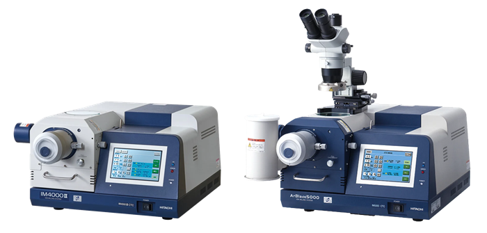
Image Credit: Hitachi High-Tech Europe
Overview
The Hitachi IM4000II and ArBlade 5000 are high-precision ion milling systems designed for SEM sample preparation. Whether analyzing metals, semiconductors, polymers, ceramics, or layered materials, these systems are essential for producing high-quality, artifact-free cross-sections and polished surfaces.
Developed for academic research, industrial quality assurance, and materials science laboratories, both systems provide rapid and consistent outcomes, establishing them as vital tools for advanced electron microscopy studies.
IM4000II
The IM4000II is an all-in-one system designed for both cross-section and flat milling, making it a flexible and essential tool for basic sample preparation in any lab.
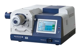
Image Credit: Hitachi High-Tech Europe
ArBlade 5000
The more advanced ArBlade 5000 offers a higher milling rate and wide-area cross-section milling. This makes it ideal for demanding applications and labs that require high throughput.
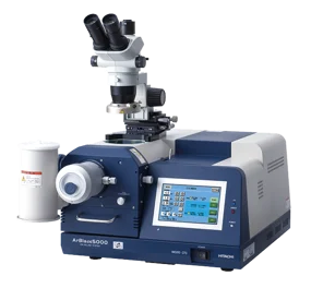
Image Credit: Hitachi High-Tech Europe
Features and Benefits
Fast and Precise Milling for a Wide Range of Materials
Both the IM4000II and ArBlade 5000 are designed to reduce turnaround times without compromising sample integrity.
- The IM4000II can achieve a milling rate of up to 500 μm/h, while the more advanced ArBlade 5000 offers a milling rate of 1 mm/h or more.
- These high milling rates make them ideal for the extended milling required for hard materials like metals and semiconductors.

Image Credit: Hitachi High-Tech Europe
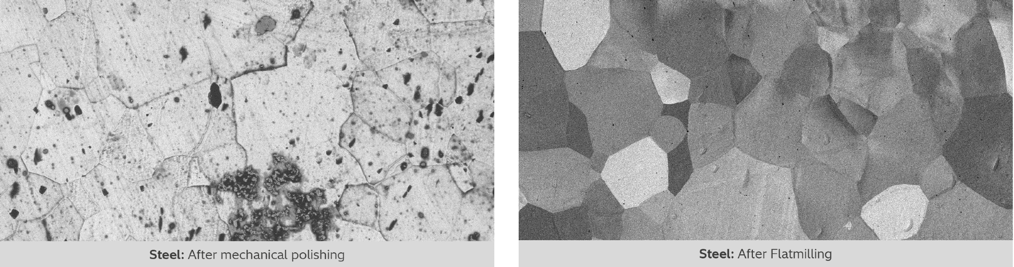
Cross-Section and Flat Milling for Flexible Sample Preparation
Prepare samples with the ultimate flexibility and control, enabling the user to meet the precise requirements of their research.
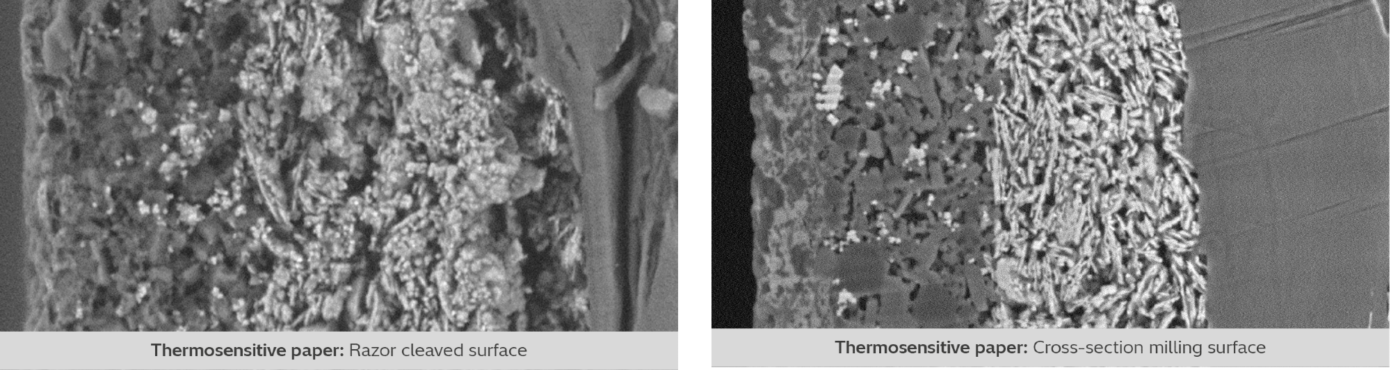
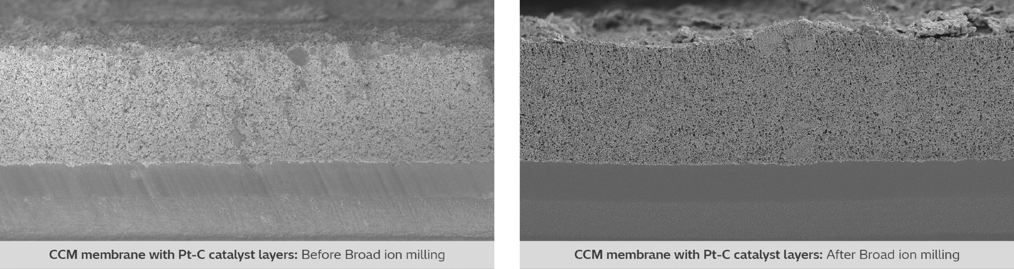
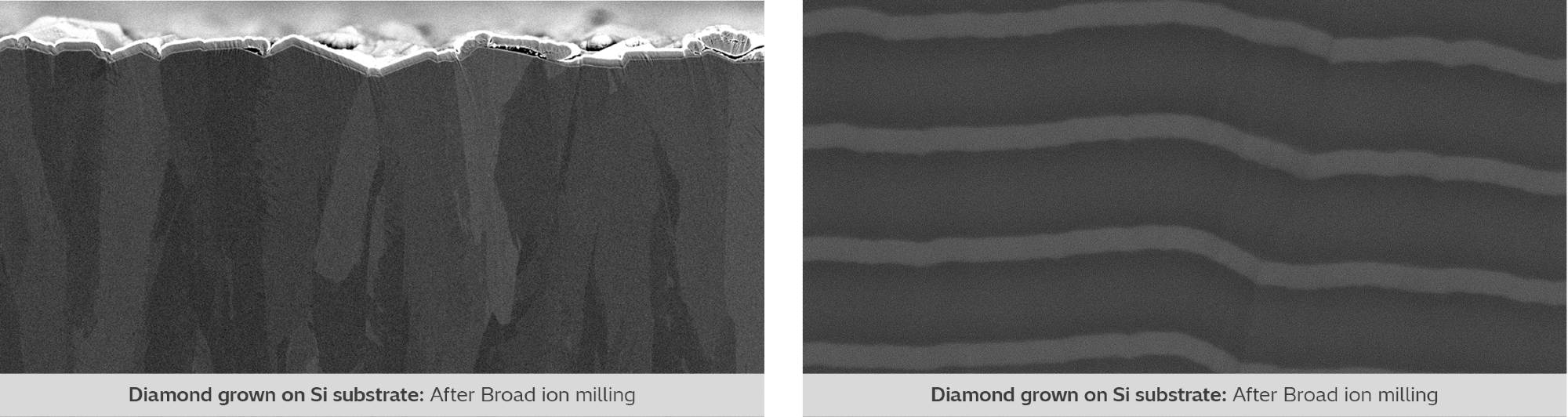
- Cross-section milling produces smooth, undistorted surfaces free of mechanical stress, making it ideal for examining the internal structures of composite materials, multilayer films, and electronic components.
- Flat milling is essential for applications like EBSD because it removes surface layer artifacts, which enables high-contrast imaging.
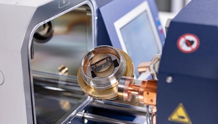
Image Credit: Hitachi High-Tech Europe
Wide-Area Cross-Section Milling (Arblade 5000 Only)
This system allows confident preparation of large samples.
- Capable of milling up to 10 mm in width, making it ideal for electronic devices and industrial materials.
- The process ensures a uniform cross-section across the entire sample, which significantly improves the accuracy of subsequent imaging and analysis.
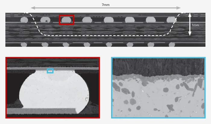
Image Credit: Hitachi High-Tech Europe
Cryogenic Cooling for Temperature-Sensitive Samples
Maintain specimen integrity during high-resolution imaging.
- An optional Cooling Temperature Control feature for both the IM4000II and ArBlade 5000 prevents heat damage to delicate materials like polymers.
- Utilizes liquid nitrogen to sustain an exact temperature range from 0 °C to –100 °C.

Image Credit: Hitachi High-Tech Europe
Seamless Integration With Scanning Electron Microscopes (SEMs)
This process ensures contamination-free imaging for air-sensitive samples.
- The IM4000II and ArBlade 5000 are compatible with both Hitachi SEMs and third-party systems, which helps streamline workflows.
- Additionally, an optional Air protection Holder Unit allows air-sensitive samples to be transferred to an SEM or AFM without being exposed to the atmosphere.

Image Credit: Hitachi High-Tech Europe
Applications
Prepare cross-sections of hard materials for microstructural analysis. Image Credit: Hitachi High-Tech Europe
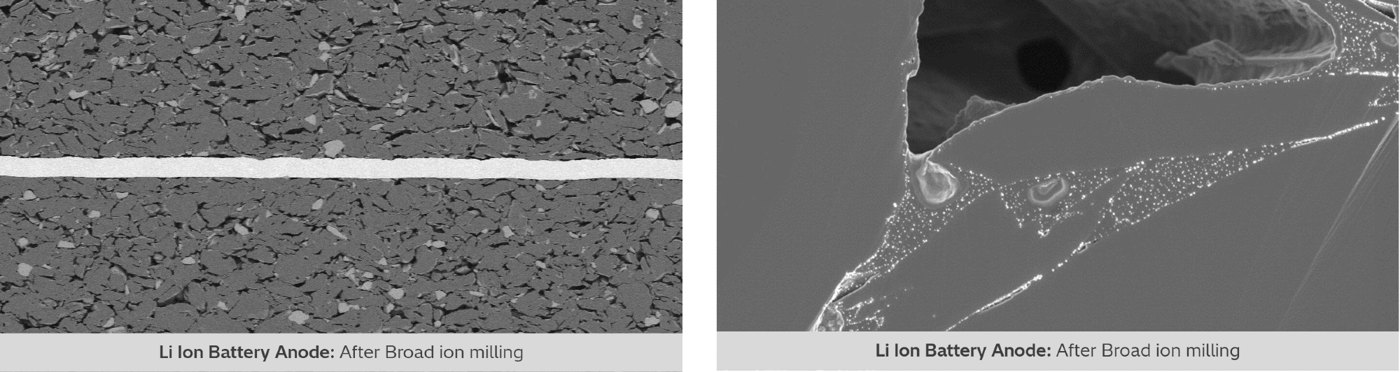
Cross-section of Li Ion Battery Anode. Image Credit: Hitachi High-Tech Europe
- Electronics and Semiconductor

Expose layers and interfaces in integrated circuit. Image Credit: Hitachi High-Tech Europe
- Polymers and Soft Materials
Prevent deformation in temperature-sensitive samples. Image Credit: Hitachi High-Tech Europe
- Multilayer Films and Coatings
Study layer composition and adhesion quality. Image Credit: Hitachi High-Tech Europe
Cross-section milling example. Image Credit: Hitachi High-Tech Europe
Specifications
Source: Hitachi High-Tech Europe
| |
IM4000II |
ArBlade 5000 |
| Gas Used |
Ar (argon) gas |
Ar (argon) gas |
| Accelerating Voltage |
0 to 6 kV |
0 to 8 kV |
| Maximum Milling Rate (estimated for Si samples and 100 μm protrusion) |
500 μm/h or more |
≥ 1 mm/h |
| Maximum Milling Width |
Not available |
10 mm |
| Maximum Specimen Size |
20(W) x 12(D) x 8(H) mm |
20(W) x 12(D) x 8(H) mm |
| Sample Moving Range |
X: ±7 mm, Y: 0 to +3 mm |
X: ±7 mm, Y: 0 to +3 mm |
| Ion Beam Intermittent Irradiation |
ON/OFF setting (1 sec to 59 min 59 sec) |
Standard function |
| Swing angle |
±15 °, ±30 °, ±40 ° |
±15 °, ±30 °, ±40 ° |
| Wide-Area Cross-Section milling |
Not available |
Up to 10 mm width |
| Flat Milling Area |
φ 32 mm |
φ 32 mm |
| Maximum Flat-Milled Sample Size |
φ 50 x 25(H) mm |
φ 50 x 25(H) mm |
| Rotation Speed |
1 rpm, 25 rpm |
1 rpm, 25 rpm |
| Tilt Range |
0 to 90 ° |
0 to 90 ° |
| Cooling Temperature Control (optional) |
0 to -100 °C via LN2 |
0 to -100 °C via LN2 |
| Higher Beam Tolerance Mask (optional) |
2x beam tolerance (Cobalt-free) |
2x beam tolerance (Cobalt-free) |
| Stereo Microscope Unit (optional) |
15x to 100x, Binocular/Trinocular |
15x to 100x, Binocular/Trinocular |