By AZoNano.com Staff Writers, adapted from material provided by the Heraeus Photovoltaics Business Unit.
Screen printing is widely used for solar-cell metallization in today’s silicon solar cell production, providing superior cost benefits when compared to other methods.
Although paste suppliers have played a crucial role in the past decade to achieve improved cell performance at a lower dollar-per-watt cost, achieving further cost reduction and cell efficiency improvement is posing a major challenge to them. Hence, it is a key priority to better understand the optimum grid pattern trend vs. cell efficiency.
H-Type Grid Pattern
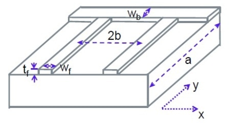
Figure 1. H-type grid pattern for rectangular solar cell
The established H-type grid pattern, shown in Figure 1, for series resistance simulation is built upon the following assumptions:
| (i) |
The cell is evenly illuminated |
| (ii) |
The photo current flows homogenously into the surface sheet and spreads laterally to the gridline and subsequently collected by bus bar |
| (iii) |
Grid line fingers and bus bar cross section area are rectangular |
| (iv) |
Fingers are uniform |
| (v) |
Finger width is 1.5 times wider than transfer lifetime (LT) |
In a practical scenario, however, screen printed fingers rarely have an ideal rectangular shape and are typically uneven. Moreover, the finger width is no longer 1.5 times wider than LT. Hence, the I-V tested series resistance values will vary from calculated values due to these discrepancies. This, in turn, results in inaccurate estimates of cell performance.
This article describes a revised model to simulate the series resistant power loss in multi-crystalline silicon solar cell designs so that the difference between the tested and calculated results is greatly reduced.
Description of Revised Model
In the revised model, the unit cell has a length of ‘a’ units and a width of ‘2nb’ units, with ‘n’ number of grid fingers at a distance of ‘2b’ from each other from their centers.
The entire rectangular solar cell is made up of repeated unit cells. The power loss caused by series resistance is related to current traversing the emitter, bus bars, gridline fingers, the contact resistance and via the base of cells.
For diffused emitter layer and base, D, the following expressions are given by Meier:
Where,
JL is the light-generated current density,
Rsheet is the emitter sheet resistance,
l is the base region thickness, and ρbase is the semiconductor base resistivity.
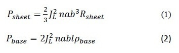
Considering the fact that the screen printed grid finger is not perfectly rectangular, a trapezoid shape or Gaussian shape is used to revise grid finger cross section area to model the practical screen printing finger shape (Figures 2a and 2b).
Figure 2. Screen printing grid finger cross-section area: (a) Trapezoid shape, (b) Gaussian shape
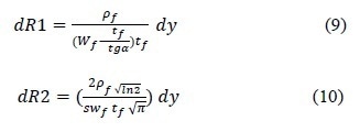
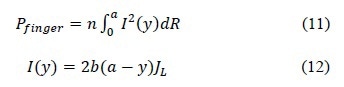
The element resistance dR of the grid finger is described as follows:
Where,
A is the cross-sectional area of the grid finger, and ρf is the gridline resistivity.
The cross section area for a trapezoid grid finger (Figure 2a) is expressed as follows:
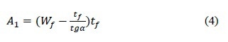
Where,
Wf is the finger width,
tf is the finger height, and t gα is the slope of finger side-wall
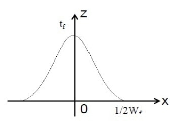
Figure 3. Gaussian profile of grid finger
The profile of a Gaussian shape grid finger (Figure 3) can be expressed as follows:
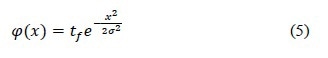
Where,
tf is the peak and σ is the standard deviation.
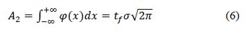
The area of the Gaussian profile can be estimated as given below:
The full width at half maximum (FWHM) is given as below:
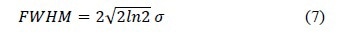
If s=FWHM/Wf, then the cross-section area can be expressed as:
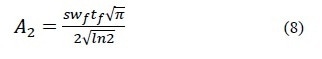
The element resistance of trapezoid and Gaussian shape grid fingers can be expressed as given in equations 9 and 10, respectively, by substituting equations 4 and 8 into equation 3.
The power loss related to the current flow through the grid finger is given as below:
The power loss of trapezoid or Gaussian shape grid fingers can be described as given in equations 13 and 14, respectively:
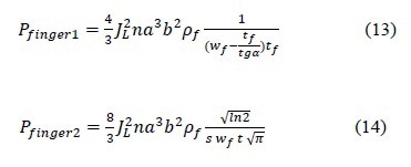
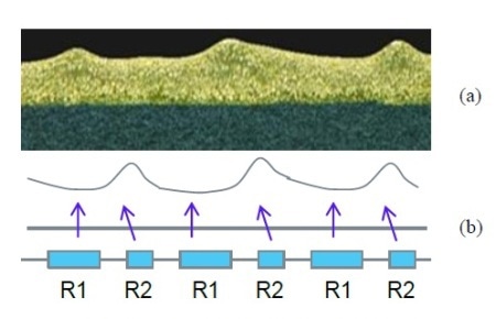
Figure 4. Resistance model for finger roughness
Uniformity is another difference between the ideal ones and practical grid fingers. Due to their roughness (Figure 4a), the line resistance of the real gridline fingers differ from that of the ideal smooth case. Since the wire mesh of the screen predominantly forms the rough surface, the valleys and peaks are comparatively regular.
If R1 and R2 represent the valley and peak areas, respectively (Figure 4b), then the resistances of a uniform and non-uniform finger are defined as given in equations 15 and 16, respectively.
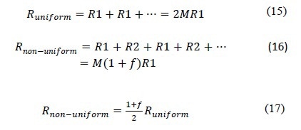
Where, f is the roughness coefficient and is expressed as follows:
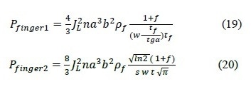
Then, the finger power loss expressed in equations 13 and 14 can be modified as given in equations 19 and 20, respectively.
Besides fingers, base and emitters, contact resistance is the fourth contribution to power loss. Then, the contact resistance based on the transfer length concept can be expressed as:
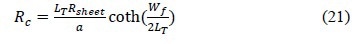
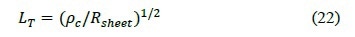
Where LT is the transfer length and is defined as below:
If Wf/2 > 1.5LT, then coth(Wf/2LT))≅ 1, and Rc=ρc/( LT α). Hence, grid width Wf does not have any influence on contact resistance. However, this limit is not valid considering the current trend to minimize finger width for mono-crystalline and multi-crystalline silicon solar cell to typically around 40∼90 µm. Therefore, there is a correlation between the contact resistance and finger width as expressed in equation 21.
Since the power loss is related to front contact resistance is 2nl2Rc, and I=JLab, then the contact resistance dissipated power yields can be expressed as follows:
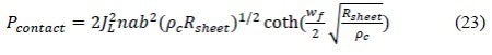
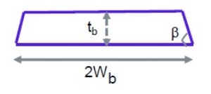
Figure 5. Cross section area of bus-bar
The cross-section area for bus-bar can be described using a trapezoid shape. Since Wb is half of bus-bar width (Figure 5) in the unit cell, the power loss of the bus-bar can be expressed as:
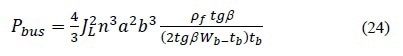
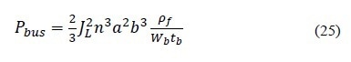
As the width of the bus-bar is much greater than that of finger, the bus-bar can be easily printed with a rectangular cross-sectional area and the resulting equation is as follows:
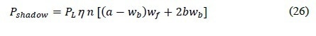
If the power density is PL and the solar cell’s energy conversion efficiency is η, the power loss caused by the front metal shadowing is:
Hence, the sum of power loss from the base, grid fingers, contact, emitter and the shadowing loss is the total power loss (equation 28).
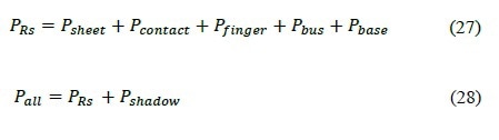
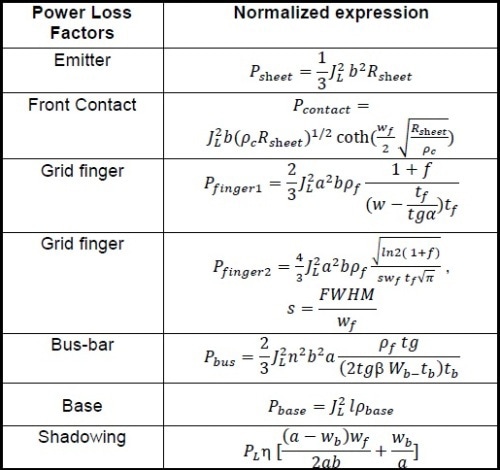
Equations 1, 2, 19, 20, 23, 24, and 26 are then normalized to unit cell area 2nab, and the summary of expressions are given in Table 1.
Table 1. Summary of Power Loss Expression
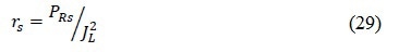
The cell series resistance, normalized to unit area, is given as follows:
Results
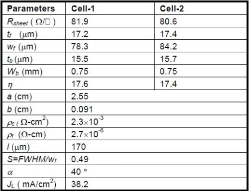
Heraeus 96XX front Ag paste was applied to print two standard multi-crystalline silicon solar cells using a 3 bus-bar 85-finger line screen and a commercial Al paste was used to form the back metallization layer. Table 2 lists the associated device and material parameters, which are used for estimating the normalized power loss factors in Table 1 as well as the corresponding cell series resistance.
Table 2. Cell 1 and 2 Device and Material Parameters
The comparison between the I-V tested values and the estimated series resistance values is shown in Table 3. The results demonstrate an increase in the calculated values, becoming closer to the tested values when the roughness effect is taken into account. Figure 6 shows the correlation between roughness coefficient f and series resistance for three types of finger models. The results clearly show the importance of finger uniformity as finger roughness influences the series resistance value, which, in turn, will affect the cell performance.
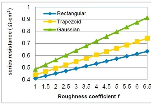
Figure 6. Series resistance vs. roughness coefficient
Finger width influence on contact resistance is depicted in Figure 7. The results demonstrate that the lesser the finger width, the larger the contact resistance. Hence, the cell performance will be greatly influenced when compared to wider fingers. Finally, different experimental pastes were used to print more samples (15 cells) to compare the resulting series resistance values with the estimated ones.
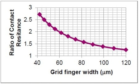
Figure 7. Finger width influence on contact resistance
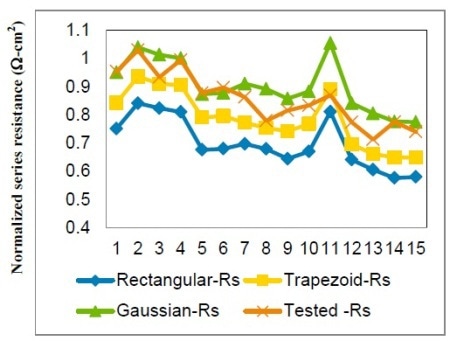
Figure 8. Estimated and tested series resistance values of 15 samples
The I-V test results and normalized cell series resistance value rs of three finger type models are depicted in Figure 8. Figure 9 summarizes the discrepancies between the tested values and the estimated results. The accuracy, which is the ratio between the estimated value and the tested value, was optimized by 10% ∼20%.
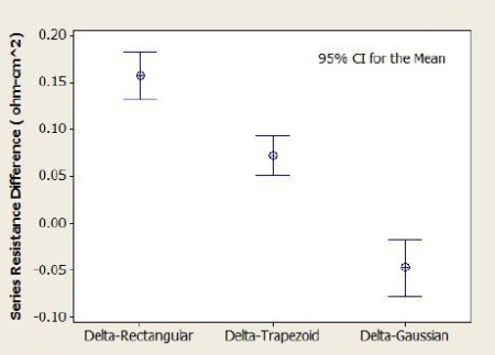
Figure 9. Interval plot of series resistance difference between tested value and estimated value
Conclusion
The following modifications are applied on traditional H-type grid pattern power loss model:
- Gaussian or trapezoid cross-section area is utilized in accordance with the practical screen printing finger shapes
- Non-uniformity effects are taken into account in the model
- Finger width influence on contact resistivity is included
The improved accuracy of the new model is verified by comparing the real I-V test data with the estimated data.
About Heraeus Photovoltaics
The Heraeus Photovoltaics Business Unit is an industry leading developer and manufacturer of metallization pastes for the photovoltaic industry.
Heraeus has been a manufacturer of thick film pastes for over 40 years. Since 2008, we have been an innovative supplier to the photovoltaics industry, working with c-Si cell manufacturers to improve their cells’ efficiency for both conventional and advanced cell designs.
Heraeus have developed silver metallization pastes that have been integrated into commercially available technologies such as MWT, Double Print, Dual Printing, Selective Emitter, Back Side Passivation and N-Type Cells.
Heraeus have also expanded our capabilities and developed lower temperature processing pastes for Thin Film and other c-Si technologies.
Heraeus' goal is to improve our customers’ cell efficiency and reduce their cell’s cost per watt through our innovative paste design technology.

This information has been sourced, reviewed and adapted from materials provided by Heraeus Photovoltaics.
For the original article, please visit Heraeus Photovoltaics.