Additive manufacturing or 3D printing is a rapid prototyping technique capable of fabricating complex 3D components directly from ceramic, alloy or metal powders. The layer-by-layer build-up process provides a range of new production possibilities, such as fabrication of complex, near net shape components with integrated functional properties, such as curved cooling channels in drills.
Powder characteristics and processing conditions greatly influence the microstructure of the components. Besides microstructural defects that are largely detrimental to the application properties of components, the following challenges need to be addressed in additive manufacturing:
- Requirement for a high level of dimensional accuracy
- Surface quality
- Fabrication of tools with complex geometries and inner structures like cooling channels
Microscopic analyses of the components produced and their microstructures help understanding the impact of process guiding better and controlling the desired quality. This article discusses the applicability of microscopic techniques to evaluate the quality of additively manufactured components.
Powder Characterization Using Optical Light and Scanning Electron Microscopy
As a powder-based process, additive manufacturing builds up components using CAD operated through layer-by-layer melting of the powder. As a result, the powder characteristics greatly influence the properties of the additively manufactured tools.
Microscopic techniques can be used to determine the tool properties. Light microscopes such as Axio Zoom.V16 can perform particle size analysis (Figure 1a and 1b). The monomodal particle size distribution of a steel powder is shown Figure 1a, whereas the bimodally distributed AlSi10 is shown in Figure 1b.
Scanning electron microscopy can be used to analyze powder morphology (Figure 1c and 1d). For instance, it is possible to detect agglomerations and the roundness of the particles, which is crucial for the powder to flow well during the process.
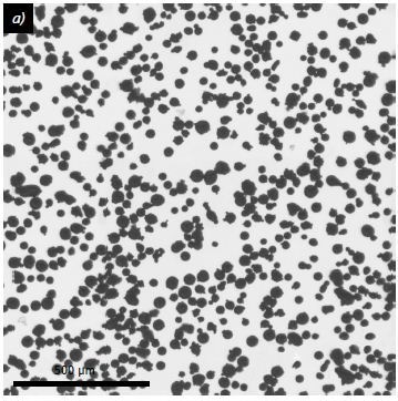
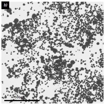
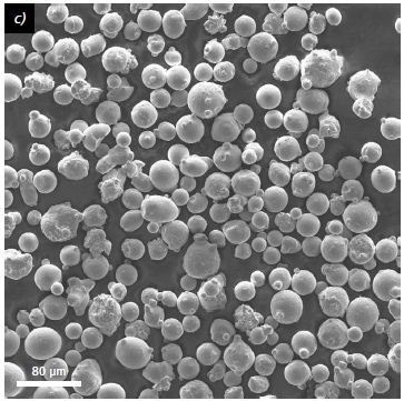
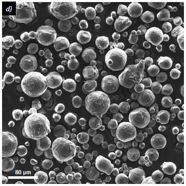
Figure 1. Micrographs of steel (316L) (a, c) and AlSi10 (b, d) Powders used for powder characterization; (a, b) Light microscopy, transmitted light, bright field, 80×; (c, d) SEM, SE, WD 10 mm, EHT 10 kV, 500×
Radiographical (CT) Non-destructive Analysis
Computed tomography (CT) is a robust technique used to examine the dimensional accuracy of additively manufactured components due to its ability to explore their inner structures. Figure 2 shows the CT comparison of a traditionally and additively manufactured steel drill, demonstrating the benefits of 3D printing.
Additive manufacturing enables the integrated fabrication of curved cooling channels. Conversely, cooling channels in conventionally manufactured drills need to be machined once the part has been finished.
Figure 3 shows the CT sections of a 3D printed drill, allowing the size measurement of inner structures such as wall thickness and dimensions and cross-section areas of the cooling channels. This, in turn, enables quality controlling.
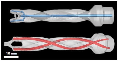
Figure 2. CT images of steel drills with cooling channels; top: conventionally produced with later machined cooling channels; bottom: additively manufactured with curved cooling channels (red).
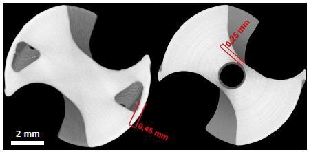
Figure 3. CT section through additively (left) and conventionally (right) manufactured drill, measuring of differences in wall thickness.
Size and Geometry of the Components
One of the key challenges in 3D printing is achieving the required dimensional accuracy. The Smartzoom 5 facilitates reviewing the size and geometry. The tip of a 3D printed cutting insert is presented in Figure 4. This micrograph is helpful to investigate the required geometry of the cutting insert such as diameter of the cutting insert, and size and location of the cooling channels.
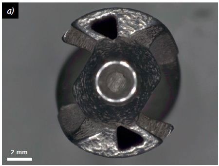
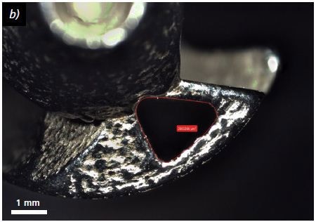
Figure 4. Size and geometry measurement with ZEISS Smartzoom 5: Tip of an additively manufactured cutting insert; a) Overview, 20×, ringlight, HDR; b) Detailed view and measurement of the cooling channel, 40×, ringlight.
Microstructural Evolution of 3D Printed Components with ZEISS Axio Imager.Z2m
The microstructure of 3D printed components can be investigated with light microscopes. Microstructural defects, phase distributions, and inhomogenities are the key aspects of interest due to their significant impact on the usage properties of the components. In addition, influences of production parameters can be observed with materialographic sample preparation followed by microscopic analyses.
The Axio Imager.Z2m light microscope can be used to illustrate the microstructural evolution of SLM (selective laser melting) processed components. The effect of the linear energy density on porosity, and the size and distribution of the pores is depicted in Figure 5. AxioVision Rel 9.1 software enables determining quantitative characteristics (fraction of porosity, area-weighted D90-distribution characteristic value of pore size).
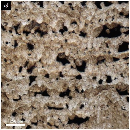
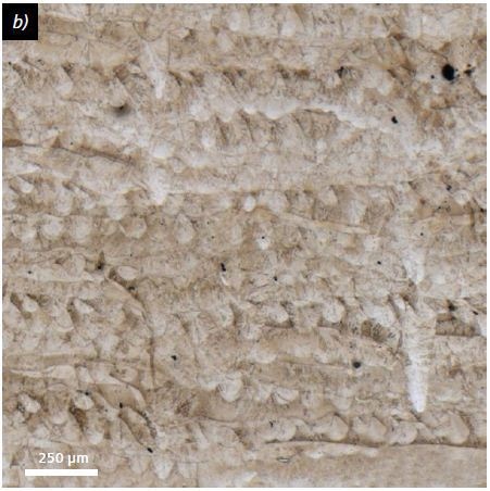
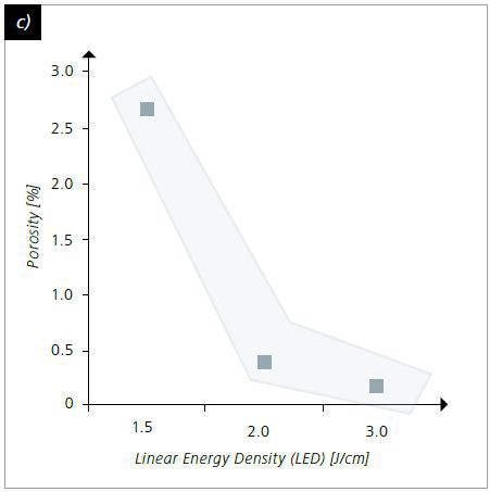
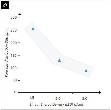
Figure 5. Microstructural evolution in test cubes made of X3NiCoMoTi18-9-5 in response to the linear energy density (LED) for determination of porosity and defect size; a) SLM, high LED, V2A etchant, cross-section, 50×; b) SLM, low LED, V2A etchant, cross-section, 50×; c) Overall porosity in relation to LED, porosity decreases with higher LED; d) Pore size in relation to LED, pore size decreases with higher LED.
Figure 6 shows the polished sections of SLM produced materials, revealing the characteristic microstructure of 3D printed samples with regular patterns caused by the process guiding. The cross-section in Figure 6a clearly shows the regular pattern of the laser tracks.
Some of the laser tracks are exemplarily sketched with white lines for better visualization. The layer construction occurring due to the individual, melted layers developing at each crossing of the laser is shown in the longitudinal section (Figure 6b).
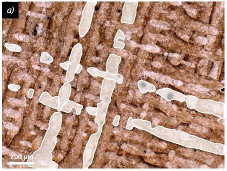
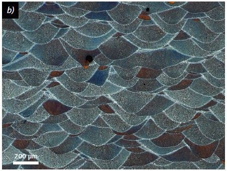
Figure 6. Microstructure formation appropriate to laser direction for SLM samples, a) X3NiCoMoTi18-9-5 (1.2709), SLM, V2A-etchant, cross-section 100×; b) AlSi10Mg, SLM, 10%-NaOH etched, longitudinal section, 100×

This information has been sourced, reviewed and adapted from materials provided by Carl Zeiss Microscopy GmbH.
For more information on this source, please visit Carl Zeiss Microscopy GmbH.