As the transistor gave rise to the information age, quantum technology has the potential to be the next great leap forward. Quantum technology is the application of quantum physics for real-world applications such as quantum computing, sensing, navigation, and communication. Here superconducting single-photon detectors (SSPDs) and superconducting qubits have been essential building blocks. The SSPDs and superconducting qubits encompass a variety of devices, including microwave resonators, transition-edge sensors (TES), superconducting nanowires for single-photon detectors (SNSPDs), Josephson junctions and high-Q superconducting resonators. One of the most crucial factors impacting the operation of these quantum devices is the choice and quality of the superconducting material used. It is important that the material of choice exhibits superconducting behavior at high critical temperatures (Tc) in order to avoid the additional cryocooler techniques that are needed for low Tc material, and that the quantum efficiency (QE) and quantum detection efficiency of these devices is maximized.1 Furthermore, it is also important that the defects in materials used in tunnel barriers, such as in Josephson junctions, are at a minimum as these could lead to decreased coherence of the qubit.2
Conventional methods for depositing superconductors include sputtering, pulsed laser deposition (PLD) and chemical vapour deposition (CVD). However, these methods can suffer from drawbacks including a lack of thickness control, poor uniformity and high impurity content. Atomic layer deposition (ALD) is much more beneficial for thin-film deposition due to its ability to produce films with high purity, precise thickness control, conformal coating in high aspect ratio structures and uniformity over large-area substrates. ALD has already successfully been applied in many fields such as in CMOS technology, high-power transistors, solar cells and many more. An emerging application is for films in devices for quantum applications. Illustrated on Figure 1 are examples where superconducting material has been integrated on to quantum nanophotonic circuitry. Figure 1(a) uses a 4 nm thick NbN nanowire folded in a meander pattern on a Si substrate with a 160 nm layer of SiO2.3 and 1(b) consists of a silicon waveguide where the detection region is covered with NbN.4 Other nitrides such as TiN may also be a possible candidate for integration in such circuitry. In this whitepaper, we focus on the potential of such superconducting nitrides by ALD.
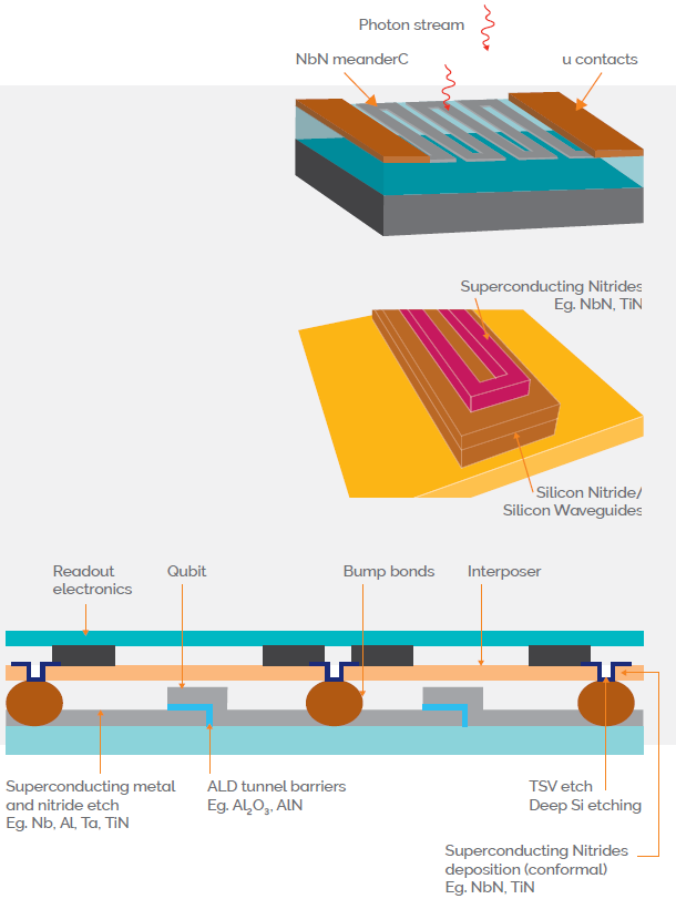
Figure 1. Fixed angle etch process flow.
 Want to know more? Click here to download the full white paper.
.jpg)
This information has been sourced, reviewed and adapted from materials provided by Oxford Instruments Plasma Technology.
For more information on this source, please visit Oxford Instruments Plasma Technology.