With maximum flexibility in precursors, process gases, and hardware design inside a single process chamber, the FlexAL atomic layer deposition (ALD) system provides a wide range of optimized high-quality plasma ALD and thermal ALD procedures.
- Maximum flexibility in the choice of precursors, process gases, hardware features, and options
- Optimized to maintain low-damage, high-quality substrates
- Removable liners enable easy chamber maintenance
- Remote plasma for low-damage plasma ALD combined with thermal ALD in one deposition chamber
- RF-biased electrode option available for control of film properties
- Industry-standard cassette-to-cassette handling for higher throughput
- Low temperature to facilitate high-quality deposition on temperature-sensitive surfaces
Overview
The ALD product line includes a variety of instruments to satisfy different needs of small-scale manufacturing, corporate R&D, and academia. There is a substantial process library at Oxford Instruments, and new processes are constantly being developed.
All ALD tools come with free lifetime process support, which includes new process recipes, guidance on creating new materials, and access to the most recent ALD process advancements.
Plasma ALD methods depend heavily on ions. Ions can enhance the quality of films, especially when used with nitrides and at lower deposition temperatures. But some substrates and interfaces could be ion-sensitive, which might harm the device.
With a sophisticated plasma source and automated matching unit (AMU), the FlexAL ALD system accurately regulates plasma ions, allowing the plasma to be used at its full potential while avoiding damage.
Features
- Chamber ports/windows for the integration of in-situ analysis equipment, e.g. ellipsometry
- Automated single-wafer load-lock for loading substrates up to 200 mm
- Clusterable with additional process modules with vacuum transfer between chambers
- Fully illustrated precursor exchange procedures with checklists
- Cleanroom interface available for through-wall installation
- Ozone generator available for integration
- Wide range of electrode options-grounded and biased electrodes
- Turbomolecular pump benefits moisture-sensitive nitrides and metals
- RF table bias option for film property enhancements such as conductivity, crystallinity, stress control
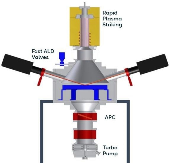
Image Credit: Oxford Instruments Plasma Technology
Applications
- Superconducting nitrides for quantum devices (e.g., TiN, NbN)
- High-quality high-k gate oxides for graphene passivation (e.g., titanium oxide, silicon oxide, gallium oxide)
- GaN HEMT pre-treatment and passivation
- ALD of 2D transition metal dichalcogenides (TMDCs)
- Pinhole-free passivation layers for OLEDs and polymers
- Passivation of crystalline silicon solar cells
- Highly conformal coatings for microfluidic devices
- ALD moisture barriers and passivation of sensitive substrates
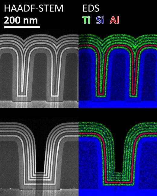
Conformal deposition of SiO2, TiO2, and Al2O3 by Plasma ALD, (CC BY 4.0 license), image library at www.AtomicLimits.com, 2021. Image Credit: Oxford Instruments Plasma Technology
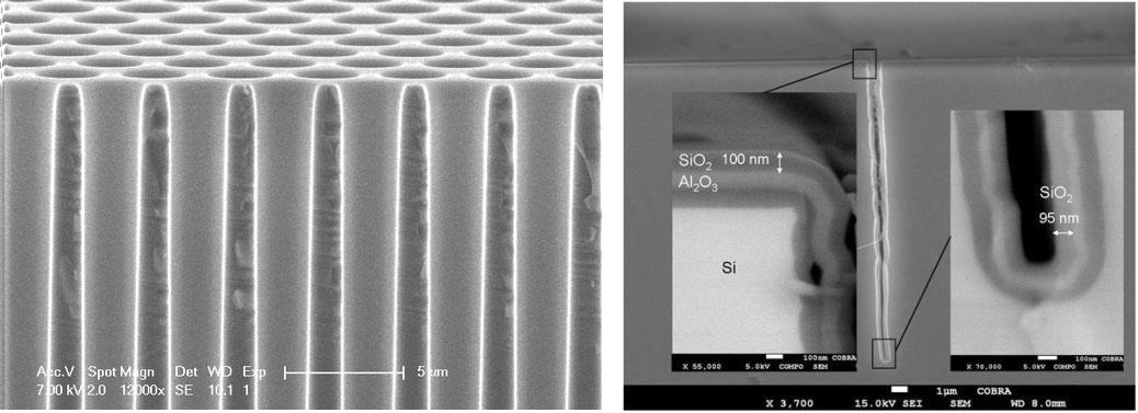
High conformality of plasma ALD Al2O3 (left image) and SiO2 (right image). Image Credit: Eindhoven University of Technology.
Specifications
- Wafer size: up to 200 mm
- Temperature range: From 30 up to 550 °C (with table bias)
- Precursors
- Precursor options for research (up to 100 g) and production (up to 500 g)
- Up to 10 plasma and thermal gas precursors
- Up to eight metal liquid or solid rapid bubbled precursors
- Ozone generator optional
- Water pot standard
- Cluster with: PECVD, ICPCVD, RIE, and Sputter modules
Options
FlexAL2D
The FlexAL2D system offers a variety of advantages for creating 2D materials and delivers ALD of 2D transition metal dichalcogenides (TMDCs) for nanodevice applications.
2D Materials Growth
- At CMOS-compatible temperatures
- Over a large area (200 mm wafers)
- With precise digital thickness control
Robust ALD Processes for 2D Materials
- Self-limiting ALD growth.
- Oxygen- and carbon-free (< 2%)
- MoS2
- High growth per cycle ~0.1 nm/cycle
- Crystalline material above 300 °C
Tunable Morphology
- Control over basal plane or edge plane orientation
- Create advanced 2D device structures
- RF substrate biasing option for film property control
- Growth of ALD dielectrics and other ALD layers on 2D materials in one tool