At the University of California/Davis, The Moulé Group is investigating the patterning and solution processing of organic electronic materials for use in equipment like chemical sensors, thermoelectric, transistors, photovoltaics, and light-emitting diodes.
The Group directly concentrates on the use of dynamic and structural measurement methods to quantify the impact of patterning and solution processing on device architecture and material morphology.
A published author and doctoral candidate with the Moulé Group, Tucker Murrey is actively developing the research and design of a scalable optical patterning process for organic photovoltaic applications.
Most working organic devices consist of several layers of material, each having a specific optical and/or electronic function. One universal design constraint for complicated device architectures, like organic field-effect transistors (OFETs), organic photovoltaics (OPVs) and red-green-blue organic light-emitting diode (OLED) displays is that they require multiple components patterned laterally and vertically to operate.
Tucker Murrey, Published Author and Doctoral Candidate, Moulé Group
Murrey continued, “Currently, many of these components are comprised of non-flexible inorganic materials. In order to move towards flexible, all organic electronic devices, there is a need to develop high precision vertical and lateral patterning methods that are compatible with solution processing.”
In the field of plastic electronics, significant research has resulted in unparalleled progress and constant improvements in organic photovoltaic (OPV) performance.
Given that conventional photolithography technology techniques are incompatible with polymeric semiconductors, there is a critical need to develop scalable photopatterning methods capable of laterally patterning organic semiconducting compounds with sub-micrometer resolution.
Tucker Murrey, Published Author and Doctoral Candidate, Moulé Group
"This patterning process would enable the construction of a sophisticated OPV architecture designed to increase external quantum efficiency. A scalable process for controlling film topography with sub-micrometer resolution would represent a substantial development that enables the advancement of complex organic electronic device architectures," Murrey continued.
Photothermal Projection Lithography
The Moulé Group is developing a range of solution-based techniques, one of which is named Photothermal Projection Lithography for Polymeric Semiconductors with Sub-diffraction Limited Resolution.
Polymeric semiconductors blend the chemical processability and mechanical flexibility of organic materials with a number of the electrical properties of inorganic semiconductors.
This allows them to be deposited from solution across large areas, which significantly decreases production costs in contrast with traditional metallic semiconductors. Developments like this have inspired a fast increase in demand for high-resolution, low-cost, and high-throughput fabrication methods.
Organic semiconductors are non-metallic materials that provide semiconductor features, whose building blocks are polymers consisting of hydrogen and carbon atoms.
These conductive polymers are electrical insulators in essence but when charges are either injected from electrodes or by photoexcitation, or doping, these polymers become conducting. Doping is where impurities are intentionally added into an intrinsic semiconductor in order to modulate its optical, structural, and electrical characteristics.
Over the past year I have been upscaling an optical patterning process that our group developed to make micro-scale electronic devices with these materials. The overall pattern area was limited to less than one square millimeter. Now we are trying to upscale the overall patterning area to about one square centimeter.
Tucker Murrey, Published Author and Doctoral Candidate, Moulé Group
An exclusive lab-scale photolithography system was designed by Murrey which modifies a Leica DM2700 optical microscope. The LED illumination source is swapped out to allow a high-powered (Class 4) 405 nm diode laser to be projected through it. An optical speckle remover, collimating lens, and a laser beam expander are all built within the system.
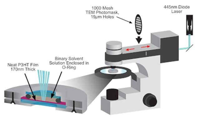
Figure 1. The lab’s unique photolithography system, modifying a Leica DM2700 optical microscope, swapping out its LED illumination source to permit a high-powered (Class 4) 445 nm diode laser to be projected through it. The laser beam is directed through a photomask pattern located inside of the microscope, then onto a semiconducting polymer film encapsulated in a sealed solvent. Image Credit: UC Davis, Moulé Group
The laser beam is focused through a photomask pattern residing within the microscope and is then directed onto a semiconducting polymer film. A sealed solvent cell comprising tetrahydrofuran ((CH2)4O) is used to contain the film, which protects the thickness of the solvent, and prevents the leaking of potentially harmful solvents. Light is projected through the mask and the objective lens is then used to project this towards the film.
The photomask comprises of glass with chrome deposits in a distinct pattern. The chrome mask is moved by the microscope into its image path so that it is in focus with the optics of the microscope. The image of the photomask is projected onto the polymer film when the laser beam is passed through it, which selectively heats the film above the polymer’s dissolution temperature and patterns the film.
"The idea is to create a light-trapping architecture in the film. The patterned features are currently sized at about 4 microns," stated Murrey, "We are currently testing to get below one micron."
This was challenging for the team, mainly due to vibration limitations.
Influence from Vibrations
A range of factors can generate vibrations that influence the sensitive micron-level instrumentation. Every structure transmits vibrations from external and internal sources. Within a building alone, the ventilation and heating system, elevators, fans, and pumps are just a few of the mechanical devices that produce vibration.
How strongly these vibration sources influence the equipment depends on how far the sensitive instrumentation is located from these sources, and where the equipment is located within the structure.
Outside of the building, the equipment can be affected by vibrations from nearby construction, loud noises from aircraft, adjacent road traffic, and even wind and different weather conditions that can cause the structure to move.
A number of these vibrations are low hertz (Hz) and are transmitted horizontally. As vibrations arising from horizontal buildings are less noticeable, vibration isolation systems usually under-compensate for this risk and they are transmitted directly to the instrumentation.
"Our lab is located on the third floor of a building on the UC Davis campus," explained Murrey, “Aside from a number of exhaust hoods which create vibration, students and faculty moving around in the building and doors slamming in hallways creates minute vibrations that interrupt our experiments."
Murrey added, "Anything that could vibrate the optics or the laser system while the pattern of the photomask is recorded on the film would blur the image. We would not be able to record fine features, and certainly not at one micron and smaller. Working at these micron and sub-micron levels our necessity for vibration isolation became critical for our optical patterning systems."
Negative-Stiffness Vibration Isolation
A Negative-Stiffness vibration isolator was chosen by The Moulé Group for its investigations. Minus K Technology developed Negative-Stiffness vibration isolation.
The company is an OEM supplier to major manufacturers of micro-hardness testers, scanning probe microscopes, and other vibration-sensitive equipment and instruments, for example when testing zero-g simulation of spacecraft.
The isolators from Minus K Technology are employed by over 300 government laboratories and universities in 50 countries.
These vibration isolators do not require compressed air or electricity and are compact, which means the sensitive instrumentation can be installed wherever a laboratory or production facility will be located. There are no pumps, chambers, or motors, and no maintenance is required as there is nothing that could wear out. They function entirely in a passive mechanical mode.
A strong advantage of Negative-Stiffness isolators is that they attain a high degree of isolation in many directions. These isolators provide flexibility where resonant frequencies to 0.5 Hz* horizontally and vertically can be customized to the application (with certain versions at 1.5 Hz horizontally).
*Note that isolation begins at 0.7 Hz and improves with an increase in the vibration frequency for an isolation system with a 0.5 Hz natural frequency. The natural frequency is more frequently employed to describe the performance of a system.
“Vertical-motion isolation is provided by a stiff spring that supports a weight load, combined with a Negative-Stiffness mechanism,” explained Dr. David Platus, President and Founder of Minus K Technology and the inventor of Negative-Stiffness isolators.
Platus continued, “The net vertical stiffness is made very low without affecting the static load-supporting capability of the spring. Beam-columns connected in series with the vertical-motion isolator provide horizontal-motion isolation. A beam-column behaves as a spring combined with a negative-stiffness mechanism. The result is a compact passive isolator capable of very low vertical and horizontal natural frequencies and high internal structural frequencies.”
Very high performance is offered by Negative-Stiffness isolators, as quantified by a transmissibility curve. Vibration transmissibility measures the vibrations that are transferred through the isolator in relation to the input vibrations. When modified to 0.5 Hz, Negative-Stiffness isolators attain an estimated 99.7 percent isolation efficiency at 10 Hz, 99 percent at 5 Hz, and 93 percent at 2 Hz.
Performance
The performance of the Negative-Stiffness isolator has provided many benefits to the laboratory. "In use for over a year now, we have not had any of our experiments interrupted by vibration issues," concluded Murrey, "We needed the vibration isolation table to isolate our optical patterning system and enable us to bring our micron-level research to the next level."
Acknowledgments
Produced from materials originally authored by Jim McMahon at Minus K Technology, Inc.

This information has been sourced, reviewed, and adapted from materials provided by Minus K Technology.
For more information on this source, please visit Minus K Technology.