Sponsored by MerckJan 4 2021
A wide variety of devices have their properties limited due to the inherent properties of the materials that they are composed of. Yet, at the nanoscale, the properties of devices no longer rely solely on the material type, but also on the geometry of the material (for instance, transforming glass into the exuberant colors of an opal). Nanowires - anisotropic structures with diameters ranging from one to hundreds of nanometers and lengths of tens to hundreds of microns - offer a novel platform for exploiting such nanoscale phenomena.
Many nanowires are individual crystals and due to their narrow diameter have an exceptionally high surface area. Subsequently, the nanowires are very sensitive to changes in surface chemistry and are prevalent in sensor development.1
Nanowire diameters are also small enough to enable damage-free penetration of biological structures, while their length allows them to transmit signals in and out of a cell.1 Thus, nanowires are very effective as battery electrodes due to these properties, with elongated conduction pathways that reach high conductivity and high surface area that enables high-speed charging.2
Some of the greatest gains produced by nanowires is the potential to exploit the properties that only appear on the nanoscale. Less than the wavelength of visible light; the diameter of a nanowire works in the waveoptics regime. By manipulating nanowire geometry to choose specific optical modes enables the tuning of absorption and reflectivity.3 Likewise, as nanowires are under the mean free path for phonons, this allows for a reduction of thermal conductivity below the bulk limit.1
The mechanical properties of nanowires also diverge from those of the bulk material due to the nanowire’s capacity to scatter strain at its surface.1 In order to generate and make use of these properties, dependable nanowire syntheses that can be controlled are necessary, but synthetic methods differ in how the exceptionally anisotropic structures are produced. In broader terms, synthesis techniques can be separated into two categories: top-down fabrication and bottom-up synthesis.
Top-Down Fabrication
The traditional top-down method of nanowire fabrication is a subtractive one, like sculpting a figurine from a block of marble, using chemicals to carve away and achieve nanoscale control. It uses several of the techniques utilized by the semiconductor industry, including lithography and chemical etching, to transform a bulk wafer or crystal into nanowire structures.
Generally, top-down fabrication depends on expensive, large and pinpoint instrumentation that can be typically found in cleanroom and nanofabrication facilities.
Lithography
Lithography is amongst the most popular top-down techniques for nanofabrication. This method is broadly utilized in the microelectronics industry. This technique demands the deposition of a resist material, such as poly(methylmethacrylate) that will resemble a photographic film to generate a pattern post-exposure and development using a patterned mask. The limited resolution of photolithography a result of the lithographic technique and wavelength of light used and is not usually suitable or practical for small nanowires.
Patterns with greater resolution can be acquired with electron-beam lithography, which is a direct-write maskless exposure technique. For the production of vertical nanowires, the pattern will be comprised of a series of circles or holes above a wafer of the target material. For horizontal nanowires, the pattern will be a sequence of trenches or lines or on a layered substrate, such as silicon-on-insulator (SOI).
The production of nanowires is made possible by etching the superfluous material from the wafer. The resist may be utilized directly as the etch mask, depending on the process, or may supply the template for deposition of a mask material with increased stability, such as gold. The pattern can be etched using wet chemical etchants, like potassium hydroxide (Prod. No. 306568), or an electrochemical etchant as shown in Figure 1A.
This technique often yields tapered as opposed to cylindrical wires due to etching underneath the mask. This issue can be significantly reduced by the use of anisotropic etchants, but it is rare to eliminate it completely.4
One approach to accomplishing the production of cylindrical vertical wires is to substitute the wet chemical etch with an extremely anisotropic deep reactive ion etch (DRIE), which can generate vertical nanowires that are tens of microns in length. Otherwise, the pattern can be inverted and metal-assisted etching used5 as demonstrated in Figure 1B, to realize relative anisotropic structures.
Other approaches to traditional lithography promise greater resolutions than can be accomplished with optical lithography. Furthermore, higher throughput is made possible with alternative methods. For example, Nanosphere Lithography (NSL) requires the self-assembly of a monolayer of polystyrene nanospheres onto a substrate in a tightly-packed lattice.6 These spheres act as a mask for the deposition of a metal or other masking material and are later eliminated after deposition.
Nanoscale patterns can also be generated via mechanical transfer using nano-imprint lithography (NIL).7 Moreover, cost-intensive techniques such as electronbeam lithography produce a high resolution master pattern - to transfer the pattern the master is then stamped into the resist material.
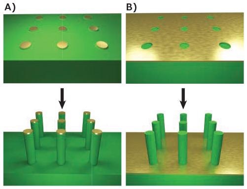
Figure 1. Top-down fabrication methods. A) Lithographic patterning of a metallic mask followed by anisotropic etching, such as DRIE. B) Lithographic patterning of exposed regions followed by anisotropic metal-assisted chemical etching. Image Credit: Merck
Benefits and Issues
Top-down nanowire fabrication is an attractive prospect due to the construction of ordered arrays of nanowires being a simple task. This enables the electrical contact to the nanowires and their incorporation into large-scale devices. In addition, several of these processes are appropriate for conventional microelectronics industry processes, meaning they can be scaled up.
However, there are some pitfalls that come with top-down fabrication. The relevance of photolithography to these processes reduces as the desired length scales decrease, necessitating the application of more progressive methods such as extreme ultraviolet (EUV) lithography. Substitute processes to photolithography, such as electron-beam and scanning probe lithographies, are direct-write methods, demanding slow serial writing of each single element. For industrial-scale production, parallelization of these techniques is necessary.
Nanowires created by top-down processes also tend to lack complex electronic characteristics. When etched from a wafer, any preferences regarding modulation of composition must be encoded into the wafer using additional methods such as molecular beam epitaxy (MBE) or encoded after growth through implantation techniques. This processing can significantly increase the material cost of nanowire devices in contrast to bottom up techniques.
Bottom-Up Synthesis
In comparison to top-down techniques, bottom-up processes are extracted from a chemist’s toolkit, where molecules are put together bit-by-bit and scaled up to generate materials exceeding the size of the average molecule by thousands of times. Bottom-up syntheses are additive, like a tree that grows from a small seed, albeit utilizing chemistry to control structure.
Vapor Phase
Using nanoparticle catalysts and gas-phase precursors, it is possible to facilitate the frequent anisotropic growth of nanowires. One of the most commonplace methods is vapor-liquid-solid (VLS) growth, wherein gaseous precursors of the preferred nanowire material, such as SiCl4 (Prod. No. 215120) for silicon, dissolve into a liquid-metal catalyst.8
As supersaturation of the catalyst takes place, crystallization of the solid nanowire occurs from the liquid catalyst, as shown in Figure 2A. This synthesis includes a chemical vapor deposition (CVD) system, in which the pressure, temperature and flow rates of precursors can be controlled. The conditions must be regulated to minimize non-catalytic growth of material the nanowire’s side, which would disturb the cylindrical geometry.
Noble metal nanoparticles typically act as the embryonic seed for nanowire growth. For the VLS process, the metal must be shaped into a liquid droplet that acts as the catalyst. In several cases, this droplet forms a eutectic composition that melts at a lower temperature than the pure metal or semiconductor material.
Yet, when synthesizing binary or ternary materials that include a low melting metal, such as Ga in GaAs, self-catalyzation of the VLS process takes place using a Ga liquid droplet that is provided at a constant rate by a vapor-phase precursor such as trimethylgallium (Prod. No. 730734).
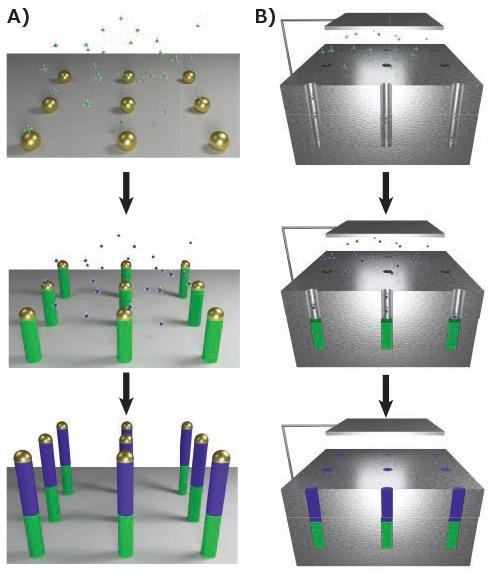
Figure 2. Bottom-up synthesis methods. A) Vapor-phase growth of segmented nanowires through the VLS process, with modulation of the gaseous precursor resulting in controlled compositional changes. B) Solution-phase growth of nanowires through electrochemical deposition into anodic aluminum oxide (AAO). A similar segmentation process is possible. Image Credit: Merck
VLS processes are beneficial because they enable compositional control. Dopant materials, such as phosphine for silicon, can be put forward and taken away repeatedly throughout the nanowire growth, generating superlattice structures with modulated electronic properties.9 Correspondingly, altering the ratio of the components in a ternary structure, like GaAsxP1–x, can create nanometer-scale bandgap modulation10 and quantumwell structures.
While metal catalysts are typically distributed on a solid substrate, an alternative called aerotaxy uses catalysts suspended in the reactor to attain high growth rates.11 A lower temperature process, known as vapor-solid-solid (VSS) growth, utilizes several of the same principles as VLS growth.12
Yet, the catalysts are solid as opposed to liquid, changing the kinetic processes. Instead of supersaturating and dissolving in a liquid, the precursors disperse through the interface between the catalyst and nanowire in order to add material. This reduces the speed of the growth process, enabling more sudden compositional changes (to the atomic level) in the nanowire.
Non-catalyzed syntheses have also been developed due to the fact if the nanowires catalyst becomes contaminated it can be detrimental to certain processes. Therefore, templated growth provides another pathway to reach the appropriate anisotropy needed for nanowires. AAO, produced by electrochemical etching, includes a honeycomb of nanometer-scale channels, providing the necessary geometry needed for generating arrays of vertical nanowires.
Traditional vapor deposition techniques (CVD, sputtering, etc.) can be utilized to pack these channels, creating nanowires when the template is removed. A patterned substrate can be used for selective area epitaxy (SAE), in which epitaxial growth takes place in regions that are exposed, but deposition onto the mask material does not materialize.13 To induce catalyst-free nanowire growth, the appearance of screw dislocations has also demonstrated itself as a mechanism.14
Solution Phase
Several methods used in the vapor phase have analogies in the liquid phase. The solution-liquid-solid (SLS) mechanism is comparable to that of VLS, with the exception of the fact nanowire precursors are diffused into a high-boiling liquid, such as squalane (Prod. No. 234311) and the catalysts are suspended therein.15 Using electrochemical deposition to fill the channels16, AAO substrates can also be used for templated solution growth, as illustrated in Figure 2B.
Calling upon the solution-phase synthesis of nanoparticles, redox reactions can also be utilized to generate nanowires.17 Seed particles are initially grown by an accelerated reduction of a dissolved precursor with a strong reducing agent like sodium borohydride. Secondary growth is attained using a more diluted reducing agent, like l-ascorbic acid, to stave off any additional seed particle production.
The nanowire anisotropy is accomplished by manipulating the surface chemistry. The inclusion of surfactants that selectively change the surface energy of particular crystal facets, such as hexadecyltrimethylammonium bromide (CTAB, Prod. No. 52370), directs growth along specific axes and subsequently producing nanowires.
Pros and Cons
Bottom-up synthesis affords the opportunity for clear regulation of nanowire composition throughout the growth process, allowing the production of complex superlattice structures. This compositional control can be utilized to encode unconventional electronic properties such as quantum well photodiodes, as well as offering a template for later processing. Therefore, a wide variety of shapes and structures that can be used in photonics, electronics and memory can be produced via the selective etching of these superlattice structures.18 (Figure 3).
The major obstacle facing further development of technologies predicated on bottom-up nanowires involves their incorporation into large-scale devices. Wires produced in vertical arrays can be used in a fashion similar to those produced by top-down methods, but several of the growth processes instead produce messy ‘forests’ of nanowires or solutions of nanowires. Recent research efforts have concentrated on the assembly and organization of the nanowires in order for them to be interfaced with traditional manufacturing steps. The synthesis of these techniques will prove critical to moving nanowires from the laboratory to the factory.
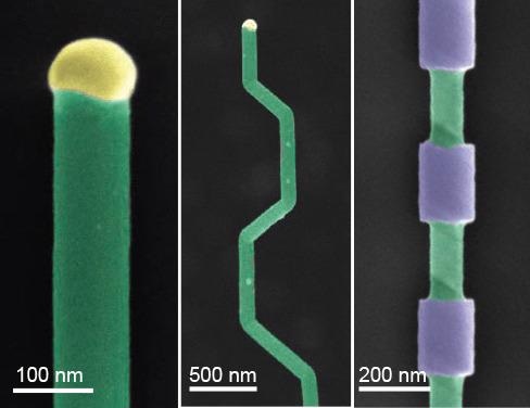
Figure 3. Nanowire structures. A) False-color SEM of a silicon nanowire grown by VLS (green) and the metal catalyst at the tip (yellow). B) Falsecolor SEM of crystallographic kinking that can be accomplished by manipulating the reaction conditions. C) False-color SEM of morphology that can be achieved by modulating the composition during growth, followed by etching. Image Credit: Merck
Conclusions
Nanowires possess many distinctive properties gleaned from their exceptionally anisotropic but often single-crystalline structure. They are extremely sensitive to any alterations in surface chemistry because of their large surface area. They also enable anisotropic charge transport, enabling accelerated radial transport or charge injection in combination with long conduction pathways along the nanowire axis.
The diameter of nanowires is small enough to allow the control of many bulk properties using the nanowire geometry. By manipulating the diameter, nanowire optical properties can be tuned which changes the optical resonant modes that can be supported by the nanowire. Correspondingly, thermal transport can be changed through nanoscale geometry. Due to their small radii, nanowires can reduce the stress more efficiently than bulk materials, making them much more pliable.
The major issue that underpins nanowire synthesis or fabrication is figuring out how to realize the appropriate anisotropy. Top-down fabrication techniques use patterning to selectively remove material to produce nanowires while utilizing bulk crystals.
In contrast, bottom-up techniques grow the nanowires from reactive precursors, using nanoparticles or nanostructured templates to generate the anisotropy. The supportive integration of top-down and bottom-up methods will be critical to the incorporation of nanowires with industrial processes. Nanowires afford an opportunity to control bulk material restrictions through nanoscale electronic and structural control, which will present the next-generation of devices and applications.
References and Further Reading
- Dasgupta, N. P.; Sun, J.; Liu, C.; Brittman, S.; Andrews, S. C.; Lim, J.; Gao, H.; Yan, R.; Yang, P. Adv. Mater. 2014, 26, 2137–2184, doi:10.1002/adma.201305929.
- Shao, M.; Ma, D. D. D.; Lee, S.-T. Eur. J. Inorg. Chem. 2010, 4264– 4278, doi:10.1002/ejic.201000634.
- Tian, B.; Kempa, T. J.; Lieber, C. M. Chem. Soc. Rev. 2009, 38, 16–24, doi:10.1039/b718703n.
- Wu, B.; Kumar, A.; Pamarthy, S. J. Appl. Phys. 2010, 108, 051101, doi:10.1063/1.3474652.
- Huang, Z.; Geyer, N.; Werner, P.; de Boor, J.; Gosele, U. Adv. Mater. 2011, 23, 285–308, doi:10.1002/adma.201001784.
- Cheung, C. L.; Nikolić, R. J.; Reinhardt, C. E.; Wang, T. F. Nanotechnology 2006, 17, 1339–1343, doi:10.1088/0957-4484/17/5/028.
- Chou, S. Y.; Krauss, P. R.; Renstrom, P. J. Science 1996, 272, 85–87, doi:10.1126/science.272.5258.85.
- Wagner, R. S.; Ellis, W. C. Appl. Phys. Lett. 1964, 4, 89–90, doi:10.1063/1.1753975.
- Christesen, J. D.; Pinion, C. W.; Hill, D. J.; Kim, S.; Cahoon, J. F. J. Phys. Chem. Lett. 2016, 7, 685–692, doi:10.1021/acs.jpclett.5b02444.
- Gudiksen, M. S.; Lauhon, L. J.; Wang, J.; Smith, D. C.; Lieber, C. M. Nature 2002, 415, 617–620, doi:10.1038/415617a.
- Heurlin, M.; Magnusson, M. H.; Lindgren, D.; Ek, M.; Wallenberg, L. R.; Deppert, K.; Samuelson, L. Nature 2012, 492, 90–94, doi:10.1038/ nature11652.
- Hobbs, R. G.; Petkov, N.; Holmes, J. D. Chem. Mater. 2012, 24, 1975–1991, doi:10.1021/cm300570n.
- Hamano, T.; Hirayama, H.; Aoyagi, Y. Jpn. J. Appl. Phys. 1997, 36, L286–L288, doi:10.1143/jjap.36.l286.
- Bierman, M. J.; Lau, Y. K.; Kvit, A. V.; Schmitt, A. L.; Jin, S. Science 2008, 320, 1060–1063, doi:10.1126/science.1157131.
- Heitsch, A. T.; Fanfair, D. D.; Tuan, H. Y.; Korgel, B. A. J. Am. Chem. Soc. 2008, 130, 5436–5437, doi:10.1021/ja8011353.
- Qin, L.; Park, S.; Huang, L.; Mirkin, C. A. Science 2005, 309, 113–115, doi:10.1126/science.1112666.
- Sun, Y.; Gates, B.; Mayers, B.; Xia, Y. Nano Lett. 2002, 2, 165–168, doi:10.1021/nl010093y.
- Christesen, J. D.; Pinion, C. W.; Grumstrup, E. M.; Papanikolas, J. M.; Cahoon, J. F. Nano Lett. 2013, 13, 6281–6286, doi:10.1021/nl403909r.
This information has been sourced, reviewed and adapted from materials provided by Merck.
For more information on this source, please visit Merck.