Chemical mechanical polishing (CMP) – also known as planarization – has long been the most commonly employed technique for smoothing and flattening wafer surfaces during the fabrication of semiconductor integrated chips (IC). This approach has been common practice for decades.
During this time, post-CMP evaluation has become the standard means of ensuring adequate planarity of IC layers, as well as the most common approach to confirming their compliance with planarity requirements.
Conventional post-CMP process evaluation methods have analytical limitations, however. Ever tightening process control limits have led to an increasing need for improved accuracy in the wafer surface characterization methods used in semiconductor chip manufacturing.
An optimal alternative to these traditional methods can be found within post-CMP assessment using advanced 3D optical profiler technology. This approach enables more timely and accurate identification of CMP integration issues, therefore reducing manufacturing costs associated with demanding contemporary IC scaling trends.
This article outlines the use of white light interferometry (WLI) for post-CMP wafer characterization, exploring how advanced packaging manufacturers and CMP specialists can acquire key data from high-resolution, full-die maps using this 3D optical profiling technique.
Metrology Considerations for CMP
Semiconductor chip manufacturers typically employ CMP to remove excess dielectrics and metal materials after deposition, as well as removing these between layers. This helps ensure sufficient levels of surface planarity for the next process step. The continuous miniaturization of IC transistors has seen CMP become one of the most essential processes in chip manufacturing.
Recent industry advancements in heterogeneous integration (such as CoWos), 3D memory stacking technology (such as NAND memory), and advanced packaging techniques have resulted in the imposition of further constraints on CMP specifications, increasingly tightening CMP process requirements.
CMP professionals and manufacturers frequently acquire localized, small-area surface topography measurements in order to assess CMP process performance. These measurements can be used for both QC and reticle inspection.
Variations in pattern density and size across the die can arise, however, prompting non-uniform planarization. Because of this, small-area measurements may not necessarily be representative of the full-die CMP topography.1
Bruker’s WLI-based 3D optical profilers are able to overcome this analytical limitation, thanks in large part to their high vertical resolution, high throughput, and areal metrology capabilities. Bruker’s WLI-based 3D optical profilers can facilitate the rapid, straightforward collection of large-area surface topography measurements (mm2 to cm2), efficiently delivering full-die maps with angstrom-level vertical resolution and micrometer-level lateral resolution. Using this information, manufacturers can ensure a more reliable assessment of wafer surface planarity and CMP process efficacy.2
Full-Die Map via Image Stitching
The primary limitations of conventional post-CMP wafer characterization stem from its inability to collect data across the full die. This creates a notable analytical blind spot, resulting in susceptibility to CMP alignment issues.
Contemporary advanced 3D optical profilometers employ precision stitching algorithms, combining multiple fields of view (FOV) in order to extend the evaluation length. These profilometers are also capable of automatic analysis, culminating in rapid, repeatable and artifact-free imaging – even when imaging wide areas.
In the example presented here, a standard 200 m test CMP wafer exhibits well-defined structures in different sizes, width and line-spacing values in order to simulate a range of topological features. This test CMP wafter was coated with a 20 nm opaque titanium layer designed to address transparency and dissimilar materials present in the wafer’s surface, helping ensure accurate results with no compromise to surface topography at the die level.3
Measurements were obtained using a Bruker InSight WLI optical metrology system. The system was fitted with an Equipment Front End Module (EFEM) to facilitate automated wafer handling, along with a Michelson interferometric 5x objective, which offered a large FOV (2.3 mm x 1.7 mm) and a 3.6 µm effective lateral resolution.
Data acquisition was completed in phase shifting interferometry (PSI) mode. This mode can achieve angstrom-level vertical resolution at a measurement speed of less than 3 seconds per measurement cycle.
It should be noted that the instrument’s automated stitching capability facilitates an extended measurement area up to several square centimeters. Fine camera alignment, precise XY motor motion and advanced topography continuity algorithms, also help ensure height measurement accuracy as low as 0.1 nm.
The InSight WLI’s high-throughput measurement capabilities allowed 130 individual images to be stitched together covering the 455 mm2 die within a 10 minute period (Figure 1). Post-processing analyses were utilized for local background shape removal, quickly and easily revealing even minimal erosion and dishing phenomena (Figure 2).
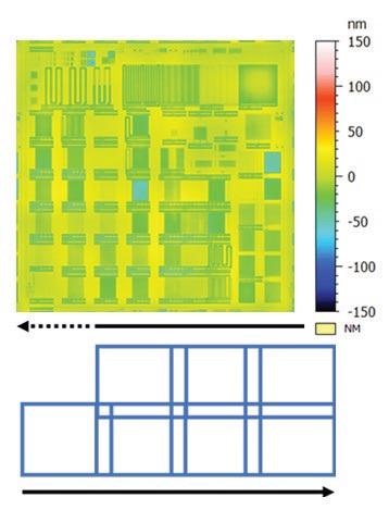
Figure 1. (a) Pattern used for die stitching individual fields-of-view; (b) Full-die map of center die (20 mm x 20 mm) from test CMP wafer. Image Credit: Bruker Nano Surfaces
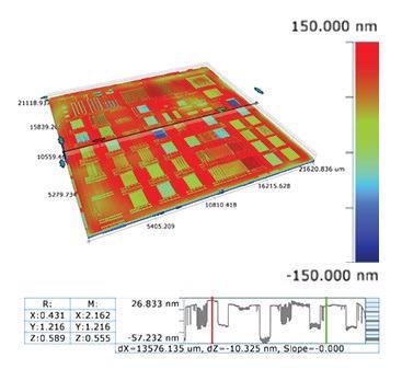
Figure 2. 3D rendering of center die at 0.25x zoom with max contrast reveals erosion and dishing in green and blue colors. Image Credit: Bruker Nano Surfaces
Post-CMP Hotspot Detection
CMP processes are highly efficient, and these are optimized for compatibility with the IC design; for example, size variation and in-die pattern density. Optimization reduces risks of “hotspot” defects that are commonly caused by under- or over-polishing at any IC layer. Risks of dishing and erosion are also reduced – two phenomena that may degrade lithographic pattern fidelity and lead to chip variability in chip performance.4 The very real consequences of these risks mean that CMP modeling for hotspot detection is an essential tool in the fabrication of high-quality and high-efficiency semiconductor chips.
Current best practices in design for manufacturing (DFM) flows involve the widespread use of CMP modeling for hotspot detection during both front end of line (FEOL) and back end of line (BEOL) processing. This process facilitates the collection of pre-CMP and post-CMP profiles from test wafers and is a fundamental consideration for manufacturers looking to build suitable models and validate modeling results.5
A range of conventional, frequently-used CMP modeling techniques exist; for example, TEM, AFM, FIB-SEM, and stylus profilometry. None of these techniques offer sufficient large-area measurement capabilities while ensuring high-resolution imaging and rapid throughput, however.6
WLI successfully connects manufacturers’ needs and these methodological capabilities, allowing users access to valuable and previously inaccessible information at full-die level when working with CMP.
In the example shown here, WLI was employed in a die-to-die comparison of planarity between test structures. These test structures were located close to the edge of the wafer and close to the center (Figure 3, top row).
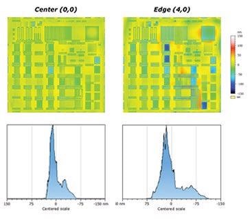
Figure 3. Top row: Die-to-die comparison of surface topography versus wafer position. Orange and blue regions emphasize issues where CMP optimization is possible. Bottom row: Respective height distribution of selected center- and edge-located dies. Image Credit: Bruker Nano Surfaces
The resulting surface map showed that test structures located close to the edge were deeper in relation to their surrounding features (illustrated by blue and dark blue tones) than structures closer to the center of the wafer. The surface maps also illustrated areas of the substrate that had a higher Z-profile (shown in orange in the figure).
These results could suggest inconsistency in the CMP process across the wafer, highlighting the need for further CMP process optimization.
Full die images can also be used to compare dies’ Z-range or height distribution, with extremes of height distributions representing effects of erosion/dishing and protrusion.
In the example shown here, WLI imaging of the full die uncovered disparate height distribution between the edge- and center-located dies, highlighting that the CMP process may have caused hotspots despite its performance at the center die (Figure 3, bottom row).
The comparison shown here has revealed information that post-CMP evaluation methods reliant on small-area “spot” measurements (for example, T-box) would likely be unable to capture or may overlook. This is because surface defects are often highly dependent on location, pattern density, and surrounding pattern structure.
Traditional in-die spot measurements may actually reinforce erroneous assertions about the fidelity of CMP integration, prompting manufacturers to pass by key opportunities to address problematic process parameters. WLI mapping provides users with access to more information at a larger scale - information that better represents the large-area interaction between the wafer and the polishing pad throughout the CMP process.
Zoom-in View on Full-Die Map
As well as facilitating imaging of the whole wafer and evaluation of the full die, WLI profilers can also preserve the lateral resolution of the images as users zoom in on smaller sections of the full-die map.
This functionality allows users to more closely examine particular areas of interest revealed by full-die mapping – for example, CMP hotspots – allowing them to better comprehend structure density’s effect on CMP process efficacy.
In the example presented here, closer examination of test structures (Figure 4) confirmed that post-CMP topography was variable dependent on motif position within the die and also on structure type; for example, pad, dense or distant lines.
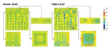
Figure 4. Zoomed-in views at different locations on the full-die map with the same vertical scale (-150 nm; +150 nm). Image Credit: Bruker Nano Surfaces
Comparisons were conducted between single-FOV horizontal profiles of the same edge- and center-die locations that had been measured using a 5x interferometric objective. These confirmed that the trench depth of the center die reached 48.2 nm, while the edge die trench was almost twice as deep, measuring 94.3 nm (Figure 5).
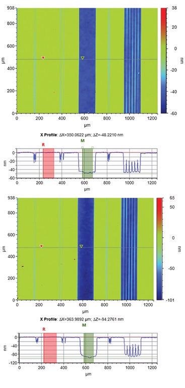
Figure 5. Single FOV image comparison between center die (top) and edge die (bottom). Image Credit: Bruker Nano Surfaces
Quantifying these defects provides useful information that can be used to predict when and where a variety of CMP process parameters must be improved; for example, material selection, pressure settings, speed settings and wafer internal stress.
High-resolution WLI imaging can provide invaluable insight into CMP results, allowing manufacturers to easily address experimental plans to optimize processes while directing users towards specific, actionable solutions that can enhance performance and yield.
Importance of Specialized Software
Bruker’s 3D optical profilometers’ distinct imaging capabilities are further augmented by the industry leading Vision64® software integration, which offers automated WLI imaging and analysis.
This software allows users to simultaneously capture a range of surface characteristics (for example, area, lowest depth, highest peak, volume, etc.) for each identified region. It also allows users to define custom measurement thresholds, flagging areas of the test structure which fail to meet set tolerance criteria.
The Vision64® software can take wafer coordinates of an identified region and utilize these to either program a high-resolution single-FOV imaging routine or export these into a coordinate map file which can be used for defect review by atomic force microscopy.
The software’s automation recipe may include more than 100 measurement locations for each die and can imagine with a high numerical aperture (NA) objective for lateral resolutions down to 380 nm.
Bruker’s AcuityXR advanced image processing algorithm can resolve 200 nm line spacing (Figure 6), further enhancing the lateral resolution. In-die stitching can be automated with a high NA objective, extending the area of measurement while making best use of the high lateral resolution.
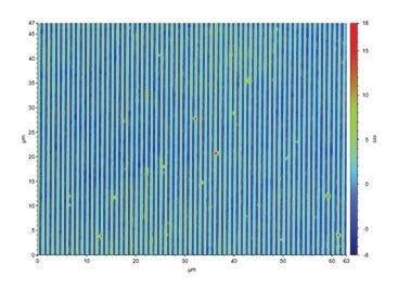
Figure 6. Single FOV image with 50x objective and 2x zoom lens on a test structure (line width/spacing - 0.5 μm/0.5 μm). Image Credit: Bruker Nano Surfaces
High-Precision, Full-Die Surface Topography Measurements
Nanometer-level deviation in surface planarity must be identified and corrected in order to ensure the success of die-to-die or die-to-wafer bonding. This is also the case for each IC layer. If full die mapping is to be a reliable tool for process optimization and an effective means of post-CMP wafer surface evaluation, it is imperative that WLI imaging results consistently realize 1 nm accuracy.
Repetitive static post-CMP evaluation experiments coupled with close monitoring and comparison of data can provide an enhanced understanding of the accuracy and repeatability of full-die measurements.
In the example presented here, a total of 10 static repeats were performed on the center die while both the Z-height distribution and the mean roughness of the resultant full-die maps were monitored (Figure 7).
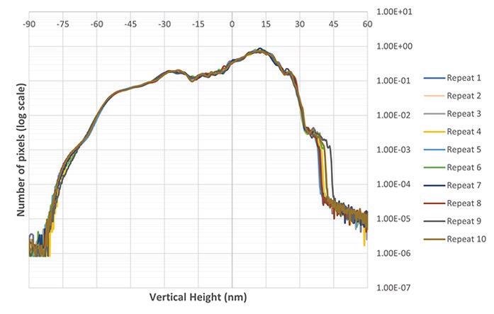
Figure 7. Z-height distribution in log versus linear scale on 10 static repeats. Mean roughness reaches Sa = (15.9 ± 0.1)nm. Image Credit: Bruker Nano Surfaces
This short-term repeatability test returned excellent results, both qualitatively and quantitatively. Full-die mapping produced an identical CMP fingerprint on every test feature, while the results displayed a near-identical height distribution in each instance.
Despite the small sample size, agreement between test runs shows an extremely high level of repeatability. It should also be noted that long-term reproducibility on a reference QC wafer has previously been observed in actual conditions, offering repeatability of ±1 nm over the course of a year.
Conclusion
Bruker’s advanced WLI-based 3D optical profilers can confidently measure die-scale (mm2 to cm2 area) nanotopography of semiconductor IC wafers and reticles. These instruments can accomplish this with high vertical and lateral resolution and short measurement times of approximately 10 minutes.
Automated measurement and analysis routines ensure the productivity, consistency and high-level throughput necessary for contemporary imaging, advanced packaging, and NAND memory processes.
This array of features allow Bruker’s WLI technology to offer an ideal solution for CMP process design validation while facilitating improved process yield in the research and development phase. Bruker’s WLI technology is also a good option for process control in production environments.
Acknowledgments
Produced from materials originally authored by Roger Posusta and Samuel Lesko from Bruker’s Nano Surfaces and Metrology Division.
References
- F. Dettonia, M.Rivoirea, S.Gaillarda, O.Hinsingera, F. Bertinb, and C.Beitiab,“High resolution nanotopography characterization at die scale of 28 nm FDSOI CMOS front-end CMP processes,” Microelectronic Engineering 113, January 2014, pp 105-108.
- R. Posusta and S. Lesko, “Characterization of CMP Processes with White Light Interferometry,” Bruker application note #564, 2020.
- F. Dettoni et al., "Interferometry: a direct die level characterization technique," ICPT 2012 - International Conference on Planarization/CMP Technology, Grenoble, France, 2012, pp. 1-6.
- D. Woodie, Chemical Mechanical Polishing (CMP), Cornell NanoScale Facility, Cornell University 2007.
- R. Ghulghazaryan, J. Wilson, and A. AbouZeid, “Creating An Accurate FEOL CMP Model,” Manufacturing, Packaging & Materials, Semiconductor Engineering, October 20, 2016.
- C. Beitia, “Challenges in Nanotopagraphy Measurements at Die Level,” FCMN, Monterrey, California, USA, March 21-23, 2017.

This information has been sourced, reviewed and adapted from materials provided by Bruker Nano Surfaces.
For more information on this source, please visit Bruker Nano Surfaces.