Photonics-based laser accelerators are proving to be promising candidates for future particle accelerators. Photonics-based laser accelerators have the potential to reduce the size of large radio-frequency accelerators by one to two orders of magnitude – a vast improvement over current instruments.
This reduction in size could lead to compact high-energy electron sources being a viable option for a range of applications in high-energy physics and medicine.
Research is currently ongoing at the Friedrich-Alexander University of Erlangen-Nuremberg, which aims to advance the development and viability of this new kind of laser-powered accelerator.
The research team is employing silicon as the substrate material and using a top-down approach to fabricate a range of desired structures.
The fabrication process is comprised of two key steps: electron beam lithography is utilized as a high-resolution patterning technique, while inductively coupled plasma reactive ion etching (ICP-RIE) is employed as an anisotropic etching technique to transfer the patterns into the substrate.
Patterns are written on a negative tone resist, offering relatively good etching durability. After the resist has been developed, the silicon substrates are etched using a PlasmaPro 100 RIE Oxford Instruments etcher. This is done using SF6 and O2 as the etching components.
Maintaining precise control over the ratio of the two gases is important if perfect anisotropic etching with high selectivity is to be ensured.
The etching begins by igniting a stable plasma in the chamber, and once this plasma is formed, radicals begin accelerating towards the substrate. Fluorine and oxygen radicals will interact chemically with the silicon substrate, resulting in the formation of a passive layer of SiOxFy.
This passive layer prevents lateral etching throughout the process, but an optimized ratio of SF6 and O2 is still essential to maintaining a balance between the passivation rate and the etching rate.
An etching process has been developed, which offers an etch rate of 32 nm/s for flawless anisotropic etching and smooth sidewalls. This process results in 3 µm tall silicon structures with an aspect ratio of 20 - ideal for photonics-based particle acceleration experiments.
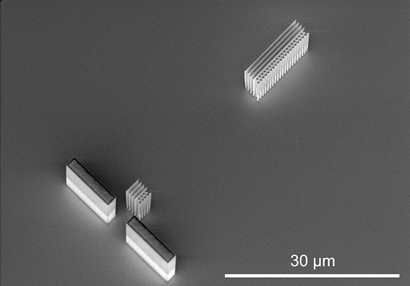
Figure 1. A two-stage silicon accelerator device fabricated by electron beam lithography and inductively coupled plasma reactive ion etching (ICP-RIE). Image Credit: Oxford Instruments Plasma Technology
Figure 1 displays a two-stage silicon dual pillar accelerator fitted with Bragg reflectors. This instrument is comprised of four solid walls, left of the dual pillar photonics accelerator structure in the upper right. An aperture is available in the front, which has been etched for alignment purposes.
This device is able to deliver accelerated electrons with attosecond pulse durations. The device’s structure, coupled with its potential for attosecond electron bunch generation, represents a huge step forward in the development of an on-chip laser-driven particle accelerator.
Acknowledgments
Produced from materials originally authored by Peyman Yousefi, Chair for Laserphysics at the Friedrich-Alexander University of Erlangen-Nuremberg.

This information has been sourced, reviewed and adapted from materials provided by Oxford Instruments Plasma Technology.
For more information on this source, please visit Oxford Instruments Plasma Technology.