Image Credit: Smileus/Shutterstock.com
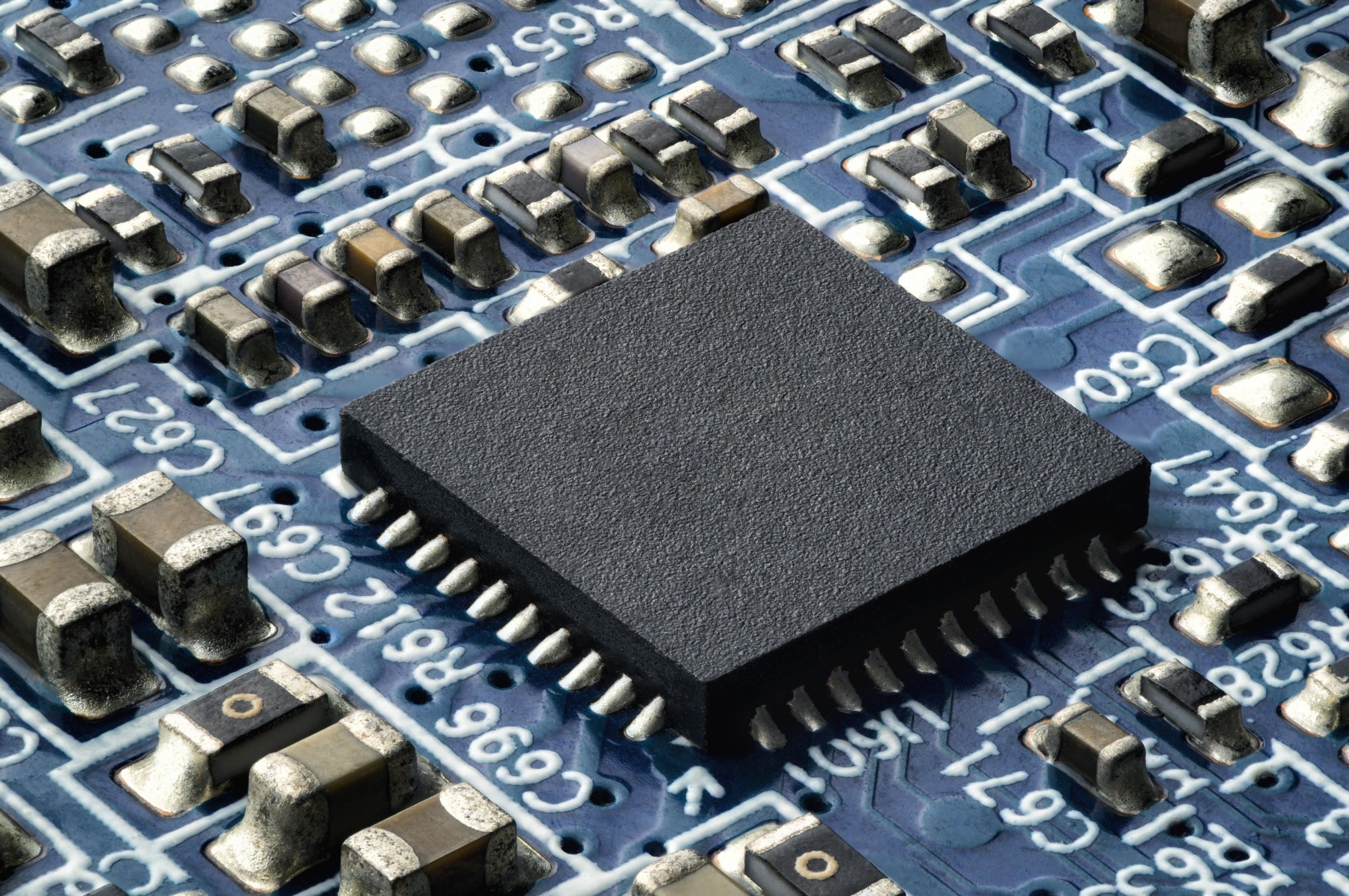
From everyday electronics like televisions and laptops to smartwatches, semiconductors have powered decades of progress. Much of this growth has been driven by continual advances in chip fabrication and packaging. However, in the era of artificial intelligence and compute-intensive applications, existing solutions still fall short of delivering the required speed and energy efficiency.
Traditional system-in-package (SiP) designs, where chips are placed side by side in a two-dimensional layout using solder bumps, face scaling and performance limitations. To overcome these, researchers at the Institute of Science Tokyo (Science Tokyo), Japan, have introduced a new 2.5D/3D integration concept called BBCube™. To move from concept to implementation, the team developed three supporting technologies, recently showcased at the 2025 IEEE 75th Electronic Components and Technology Conference (ECTC), held from May 27th to 30th.
Led by Specially Appointed Professors Norio Chujo and Takayuki Ohba, the team at the Institute of Integrated Research’s WOW Alliance Heterogeneous and Functional Integration Unit began by addressing the constraints of solder interconnects.
They developed a face-down chip-on-wafer (COW) process using inkjet printing and selective adhesive coating, enabling precise sequential bonding of chips of various sizes onto a 300 mm waffle wafer. The result was a compact 10 μm chip-to-chip spacing and ultra-fast mounting times under 10 milliseconds.
More than 30,000 chips of various sizes were fabricated onto the waffle wafer, achieving enhanced bonding speed without any chip-detachment failures.
Norio Chujo, Professor, Institute of Integrated Research, Institute of Science Tokyo
To support this high-speed COW process, the team tackled thermal stability challenges inherent to stacking ultra-thin wafers. They engineered a novel adhesive, ‘DPAS300,’ with an organic–inorganic hybrid composition. Designed for both COW and wafer-on-wafer (WOW) processes, DPAS300 demonstrated excellent adhesion and thermal resistance during tests.
Pushing further, the researchers implemented a 3D xPU-on-DRAM architecture enhanced by a new power distribution framework. This included embedding capacitors between logic and memory layers, redistributing electrical paths across the wafer, and inserting through-silicon vias (TSVs) in wafer lanes and DRAM scribe lines.
“These innovations reduced the energy required for data transmission to one-fifth to one-twentieth of that in conventional systems, while also suppressing power supply noise to below 50 mV,” stated Chujo, emphasizing the benefits of this 3D stacked computing architecture.
Collectively, these innovations represent a significant step forward in chip integration for next-generation computing systems.