Semiconductors, often known as computer microchips or integrated circuits (ICs), are an integral part of digital equipment from computers to household appliances to diagnostic instruments and military systems. This article provides a thorough background regarding the doping of semiconductors and the latest research in this sector.
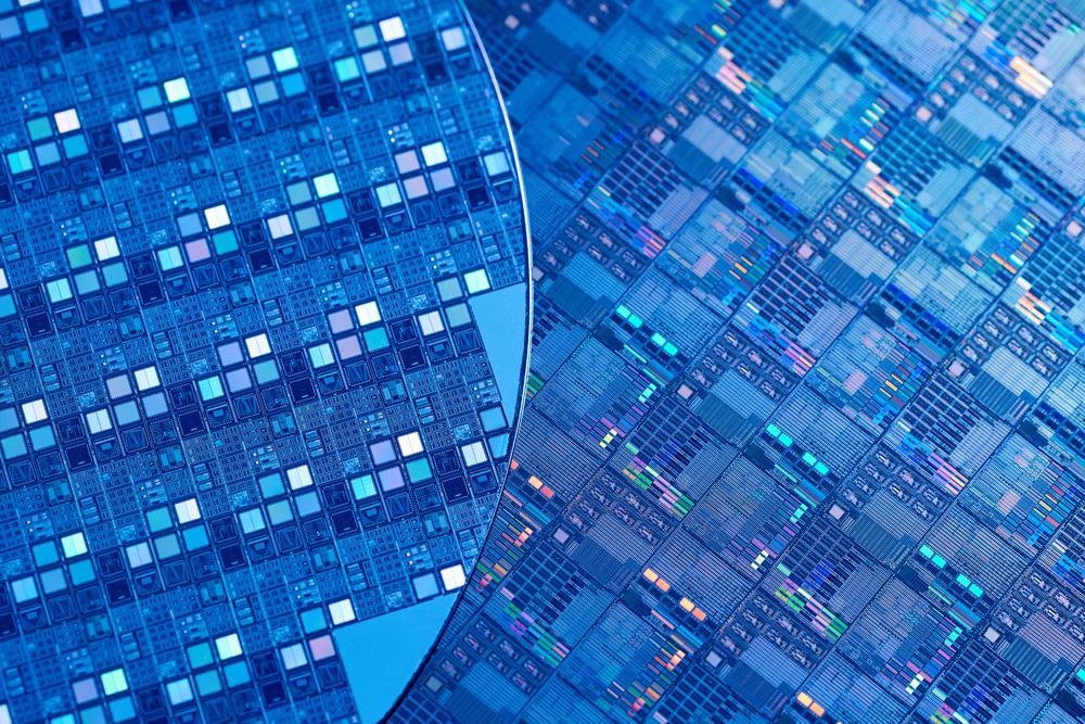
Image Credit: fotografos/Shutterstock.com
The merging of impure particles in a pristine semiconducting material is known as doping. The impure atoms here allude to those that vary from the pure semiconductor.
Doping allows researchers to manipulate the conductance of a semiconductor by utilizing the characteristics of a group of elements known as dopants. By incorporating a limited number of appropriate alternative particles, semiconductor conductance may be considerably increased.
Types of Doping
There are two different types of doping processes that are conducted using different types of dopants. These are known as n-type and p-type doping, and the dopants used in these processes are referred to as n-type dopants and p-type dopants.
How to Generate an N-Type Semiconductor
When a semiconductor, such as a group IV element silicon (Si), is doped with arsenic (As), a pentavalent n-type dopant from group V containing one more valence electron than the pure semiconductor, the impurity acts as an electron donor. When this happens, a dopant atom substitutes a silicon particle in the structure, introducing an additional valence electron into the lattice. This fifth valence electron generates an excess of electrons.
An n-type semiconductor is formed when a few particles of the impurity replace original semiconductor atoms in the lattice. The newly formed semiconductor conducts current better than the pristine semiconductor. The excess electrons are situated in high-energy valence shells, with little energy required to shift them towards the conduction band.
How to Generate a P-Type Semiconductor
The addition of a p-type trivalent group III dopant (such as boron, B) to semiconductor material allows the dopant to work as an electron acceptor because it has one fewer valence electron than the semiconductor.
When a few trivalent dopant atoms substitute semiconductor atoms in the lattice, an electron-hole is generated that may operate as an electron carrier within the lattice, resulting in a p-type material. P-type semiconductors are distinguished by a lack of negative charges and positive holes, which has the same effect as a positive charge excess. These positive holes receive electrons, increasing the semiconductor's ability to conduct current.
Can N-Type and P-Type Semiconductors be Used Together?
When a p-type semiconductor is linked to an n-type semiconductor in a suitable manner, the region of contact is referred to as a pn–junction. Semiconductor p-n junctions are used in a variety of electrical devices, such as transistors, electronics, LEDs, and solar systems.
The movements of holes and electrons generate fixed negative and positive charges, respectively. The existence of these unpaired electrical charges generates an electric field within the junction. The depletion area is the region that encompasses these charged particles (as well as the minimal number of mobile electrons or holes).
What are Different Methods of Semiconductor Doping?
Diffusion and ion injection are two of the most prevalent doping procedures.
The movement or travel of the impurity atoms from a high concentration area to a low concentration area is referred to as diffusion. Pre-deposition and drive-in are the two stages through which the process takes place.
The impurity dopant is introduced to the wafer foundation during pre-deposition. Pre-deposition is carried out on a burner at temperatures ranging from 1000 to 1250oC. The dopant, which can be in the form of a gas, solid, or liquid, is injected into the furnace.
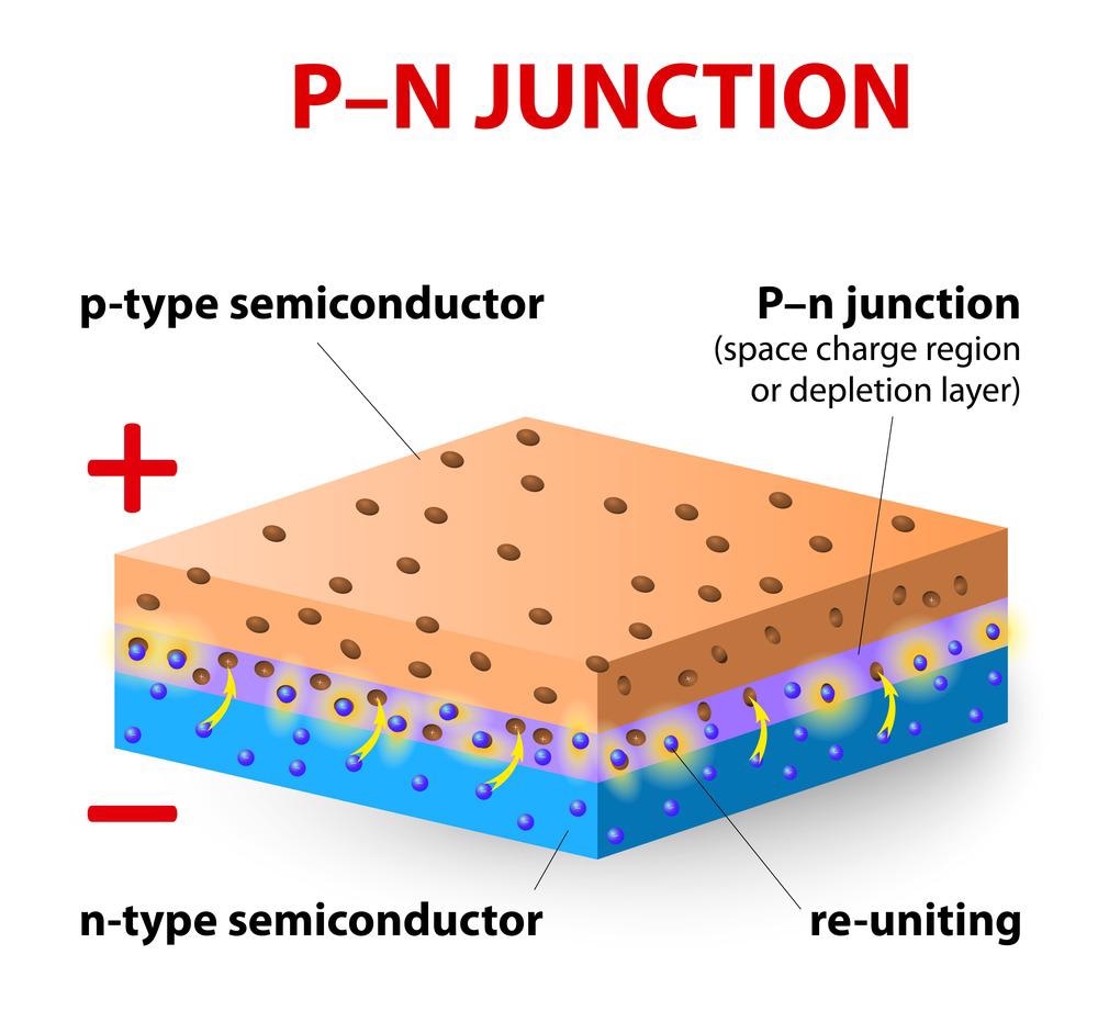
Image Credit: Designua/Shutterstock.com
The wafers are then placed in a second furnace at a higher temperature (about 1300oC) to "drive in" the additive atoms. The drive-in operation is often carried out in an oxidizing environment, resulting in the formation of a protective barrier of SiO2 over the dispersed surface.
The Process of Ion Implantation
Ion implantation involves ionizing (removing electrons from dopants), accelerating them with an electromagnetic field, and depositing them on a silicon substrate. The dopant is inserted at different depths dependent on its mass and energy when it strikes the wafer.
The exterior surface of the wafer may be damaged as a result of implantation. To restore the semiconductor to its unaltered condition and further integrate the dopant particles into the silicon crystal lattice, a high-temperature annealing stage (800-1000oC) is conducted. Annealing can be done using stacked ovens, and a high-energy laser.
Limitations
The doping process is advantageous for the electrical conductivity process; however, the emission of infrared (IR) radiation is a major drawback. Another major hazard that the operator must be careful about is the danger of thermal burns due to the high temperature of operating devices. Standardized safety measures must be ensured to maintain the safety of the user from toxic byproducts.
Latest Research
Researchers from Korea have published their research in the journal Nanomaterials, which is focused on the latest advances in the field of 2D semiconductor doping. Emulsification and synthesis advancements have allowed for the creation and electrical characterization of numerous nanoscale sheets of semiconductor transition metal dichalcogenides (TMDs).
The technique for doping nanoscale 2D semiconductor materials is comparable to that used for silicon, however, its operating mechanism has a slight variation. When it comes to doping approaches that complement doping-induced bandgap alteration, straining phenomena should be taken into account without a doubt. One of the most recent publications demonstrates that bandgap manipulation in TMD semiconductor materials is possible.
Simultaneously, in this doping-induced energy bandgap manipulation paradigm, the interface stability should be iteratively investigated since an increase in the instabilities of the interface conditions results in a decrease in carrier mobilities. These two practical challenges may be probed more deeply than ever before in terms of ICs and system-level applications.
Future of the Semiconductor Industry
The semiconductor industry perspective by Deloitte estimates the global IC semiconductor industry at US$600 Billion. The chip scarcity over the last two years has resulted in revenue losses of more than $500 billion. New technologies, such as precise deposition-enabling innovation, will enable producers to be even more exact in what they deposit on a wafer. Fluid technologies will have to become much more accurate to handle this.
More from AZoM: How is the Digital Transition Benefiting the Planet?
References and Further Reading
Deloitte. 2022. 2022 semiconductor industry outlook. [Online]
Available at: https://www2.deloitte.com/us/en/pages/technology-media-and-telecommunications/articles/semiconductor-industry-outlook.html
Yoo, H. et. al. 2021. Recent Advances in Electrical Doping of 2D Semiconductor Materials: Methods, Analyses, and Applications. Nanomaterials. 11(4). 832. Available at: https://www.mdpi.com/2079-4991/11/4/832
Halbleiter. 2022. Fundamentals: Doping: n- and p-semiconductors. [Online]
Available at: https://www.halbleiter.org/en/fundamentals/
Gupta, G., Rajasekharan, B., & Hueting, R. J. 2017. Electrostatic doping in semiconductor devices. IEEE transactions on electron devices. 64(8). 3044-3055. Available at: https://doi.org/10.1109/TED.2017.2712761
Lumen Learning. 2022. Doping: Connectivity of Semiconductors. [Online]
Available at: https://courses.lumenlearning.com/introchem/chapter/doping-connectivity-of-semiconductors/
Occupational Safety and Health Administration. 2022. Silicon Device Manufacturing. [Online]
Available at: https://www.osha.gov/semiconductors/silicon/device-fabrication
Zhao, W. et. al. 2020. Chemical doping of organic semiconductors for thermoelectric applications. Chemical Society Reviews. 49(20). 7210-7228. Available at: https://pubs.rsc.org/en/content/articlelanding/2020/cs/d0cs00204f
Disclaimer: The views expressed here are those of the author expressed in their private capacity and do not necessarily represent the views of AZoM.com Limited T/A AZoNetwork the owner and operator of this website. This disclaimer forms part of the Terms and conditions of use of this website.