The functionality of compound semiconductors comes down to the structure of the layer. However, it is uncommon for the wafer to be sliced in half like a cake in order to visualize what is happening inside.
Thankfully, non-destructive metrology techniques like X-Ray diffractometry (XRD) can be used to produce accurate and exact structural metrology in this situation. Advanced capabilities that go beyond rocking curves are becoming increasingly crucial for the production of epitaxial wafers.
Compound semiconductor wafer production is still increasing as society works to realize the full potential of these materials, which have significant sustainability advantages. Enormous amounts of energy can be saved by using compound semiconductors in power converters or LEDs.
The cost of compound semiconductors is reduced as manufacturing quality improves, allowing them to be used in more electronic devices that are sold and supplied internationally.
Malvern Panalytical’s XRD offering
- The R&D to FAB configuration of MRD XL can be upgraded
- SECS/GEM compliance
- Clean room ISO 4 available
- A large application envelope with automation is available
- Global assistance with epi experience
The maturing of the compound semiconductor industry means that, for analytical XRD equipment and those who use them, XRD techniques can be used to monitor the epitaxial growth of these devices.
Method Transfer from Lab to Fab
The equipment’s performance standards in a typical fab vary from those in most research labs. The increase in the required quality benchmarks is frequently what makes the difference.
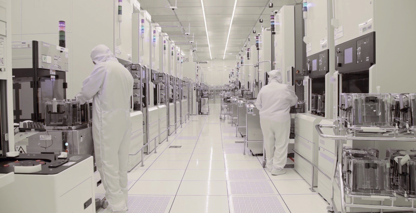
Almost all CS fabs maintain a cleanroom setting for their epitaxial department following ISO and federal classifications. To guarantee that production lines adhere to ISO cleanroom procedures and meet their yield targets, fabs must implement the most recent Semiconductor Equipment and Manufacturing International (SEMI) standards.
Parallel to this, automation is becoming more prevalent, which is understandable given the expanding size of these sectors. Automated solutions reduce the need for human interaction and contamination, making them a vital asset in semiconductor production.
A substantial initial investment may be required to set up a fab with the necessary tools, technologies, and quality controls to ensure that it functions properly. The cost of doing so might provide its own challenges.
The infrastructure for metrology tools located at R&D sites are different compared to fabrication sites. Image Credit: Malvern Panalytical
Spreading the CapEx can, fortunately, be accomplished. It becomes necessary for a compound semiconductor company to go through a development process as it grows, moving from lab techniques to fab operations.
Given the variety of possibilities available to those in charge of the tool portfolio used in the chip fabrication process, finding the best decision is a crucial, complex challenge. It is essential to understand the variables needed for each tool to achieve optimal functionality and support a seamless scaleup from research to production. It is also important that the tool will arrive on time.
By making machines futureproof and flexible, Malvern Panalytical keeps working ahead of customer needs and developments within the market, building on years of experience. Image Credit: Malvern Panalytical
Malvern Panalytical is aware of the requirements producers of compound semiconductor epi wafers and products have for their XRD solutions. Sophisticated, accurate, and precise characterization of the structural makeup of epitaxial wafers is where it all begins. In fact, it all begins with the X'Pert3 MRD XL.
The MRD XL is a global leader in X-Ray scattering applications for semiconductor manufacturers and is versatile and dependable. The company is proud to have systems that assist customers at every stage of their journey, from development to production, drawing on four decades of experience in this field.
Malvern ensures that labs and fabs working at all process phases, from research to quality control, can access high-performance tools and software packages. The MRD XL is a fully modular design in keeping with this.
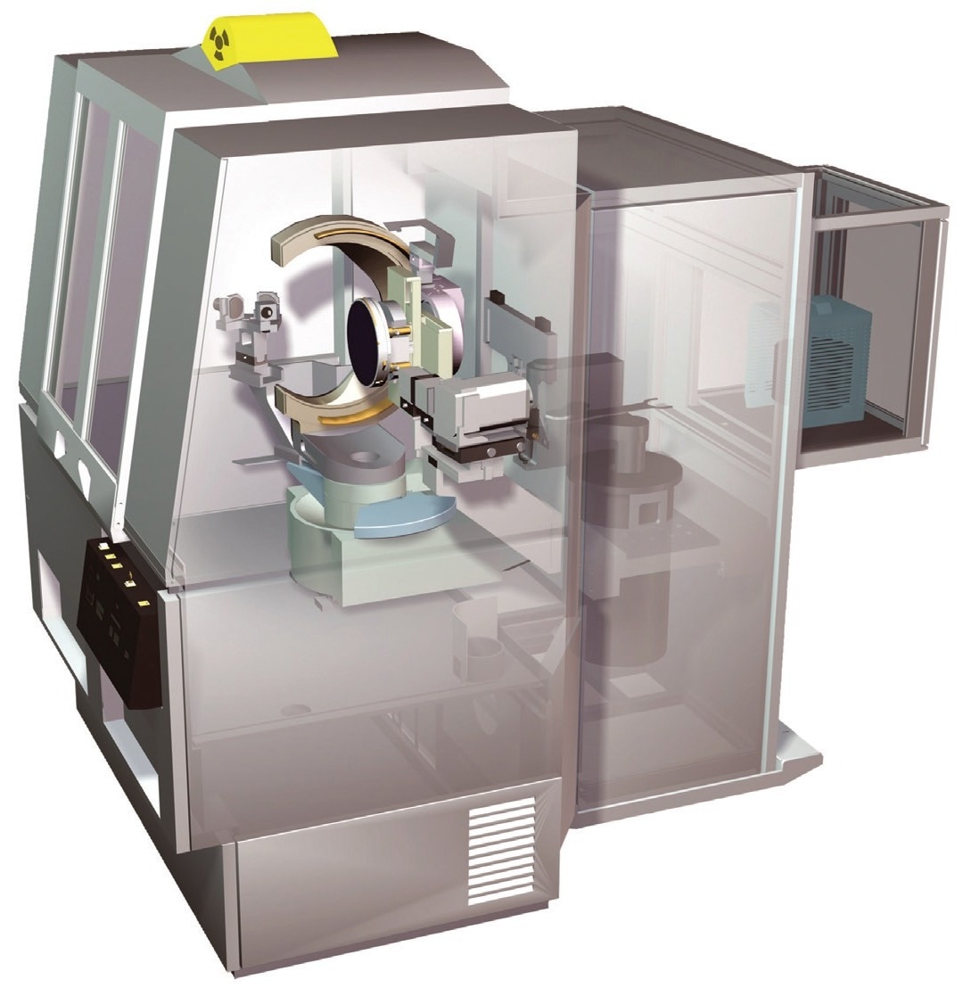
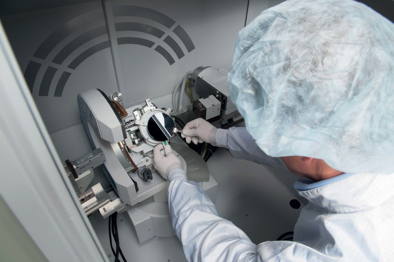
The MRD XL consists of a base module containing the measurement chamber and a front end providing the automation capability. This makes lab functionality like in-plane measurements available on the fab floor, integrated into standard recipes. Image Credit: Malvern Panalytical
By using this strategy, businesses can first acquire the core machine for R&D, then add fab components as and when their operations demand it. This method forgoes a substantial initial investment for a “fixed” solution that offers capability above and beyond what is required initially.
It is better to buy new hardware and software components that are simple to combine with the MRD XL when XRD techniques or production requirements change, such as when they need to become more automated.
A significant advantage is a metrology instrument that can adapt to a product's and its maker's expansion. This is true for small and medium-sized businesses, specialty fabs that produce multiple product lines on a single machine, and giant fabs that make product lines requiring increasingly complicated metrology.
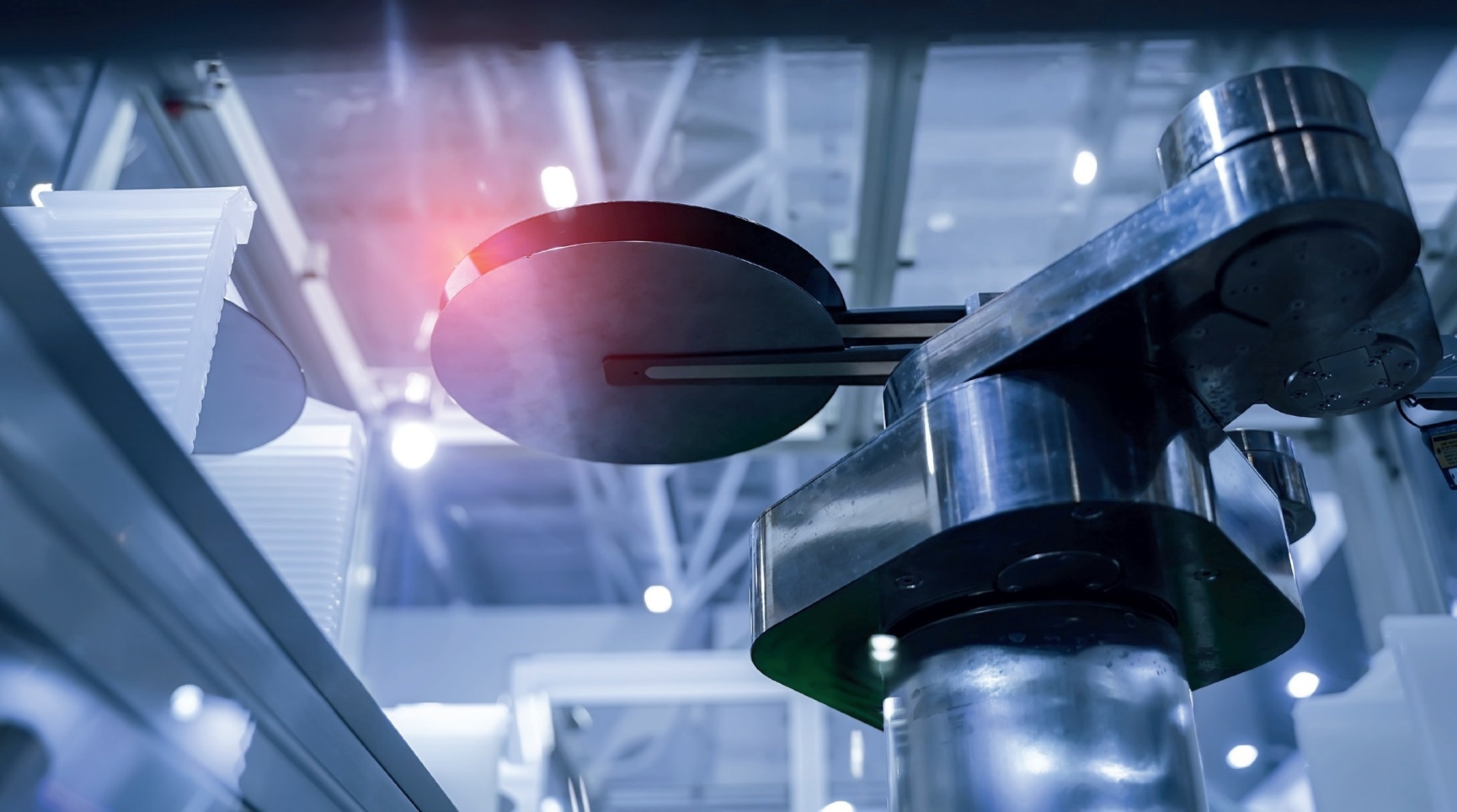
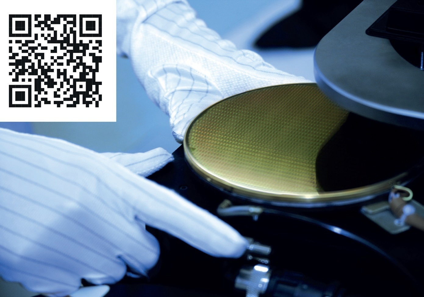
It is labor intensive to manually place wafers into metrology equipment and less reproducible than a robot with pre-aligner. Image Credit: Malvern Panalytical
When investing in an MRD XL, these companies may switch between research, pilot-scale manufacturing, full-scale production, and back. Fabrication managers have much more freedom when deciding on their CapEx budgets and timelines, thanks to the MRD XL’s incremental growth in capacity.
Automation plays a significant role in achieving the ideal cleanroom state. The significance of pertinent SEMI standards will undoubtedly increase as robotic capabilities develop, potentially reaching “lights-out” fabs with no hands-on human meddling.
More specifications will follow, including the SEMI E5 (SECS-II) and E30 (GEM) standards, which control communications between the host or carrier and the equipment, respectively. These connections, which allow the transfer of customized measurement data, are crucial to the efficiency of any semiconductor fab infrastructure.
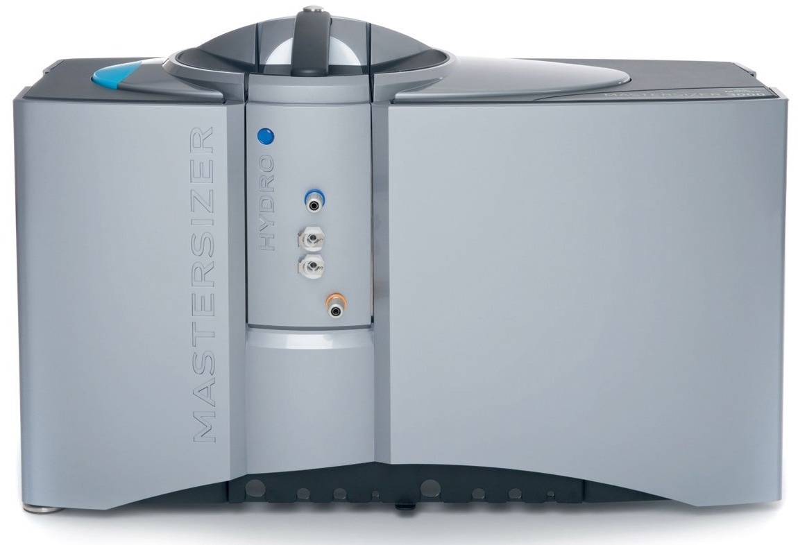
Malvern Panalytical delivers a multitude of metrology tools for the semiconductor and electronics industry such as particle characterization equipment used for CMP slurries, like the Mastersizer. Image Credit: Malvern Panalytical
Superior XRD metrology for wafer analysis is insufficient to deliver superior semiconductor materials and devices. Chemical mechanical polishing (CMP), both for substrate polishing and during processing, must be done in SEMI-standard fabs using a consistent, high-quality, and reliable method.
A wafer surface needs the proper planarity to guarantee that all the deposited layers accurately sit on one another. With the press of a button, the particle sizing products Mastersizer and Zetasizer provide precise management of slurry specifications.
Decision-makers in any quickly evolving business must consider the future or locate a dependable partner with the skills to do it for them. This is not an issue for the chip makers and developers working with Malvern, as they never have to be worried about spending money on lab-to-fab equipment that will soon be replaced by more advanced models.
Malvern’s solutions are based on years of experience and a wealth of knowledge and have been used successfully for over ten years.
Malvern Panalytical understands the full process from front-end to electronics assembly and offers more solutions, not mentioned here. Image Credit: Malvern Panalytical
Compound semiconductor advancements like lights-out fabs, the switch to larger wafer sizes, and the rising complexity of superlattices in compound semiconductors are already in the near future.
It is increasingly difficult to predict other, further advancements. Yet, Malvern is dedicated to improving and upgrading its hardware and software to ensure that these solutions – and its customers – are always ready to tackle and overcome the next challenge that comes their way.
Investments in the lab-to-fab process involve CapEx. Malvern Panalytical provides adaptable XRD solutions that may expand to meet the business’s demands.
This information has been sourced, reviewed and adapted from materials provided by Malvern Panalytical.
For more information on this source, please visit Malvern Panalytical.