Accurately controlling film thickness and uniformity is extremely important for both throughput and performance in the automotive, aerospace, semiconductor, medical, and research industries.
White light interferometry (WLI), also called coherence scanning interferometry (CSI), is the modern standard for 3D, non-contact measures of surface topography and texture.
In fact, it is the only method that delivers film thickness, coating uniformity information, and roughness of film and substrate over large areas in a single measurement, taking only a few seconds to obtain.
This article explores film thickness metrology using WLI, specifically through-film measurements of both transparent thick and thin films, as well as opaque film step measurements.
Conventional Step Measurements for Thickness
The easiest way to determine the thickness of opaque, non-transparent, and sometimes transparent films is by measuring a step from the top of the film to the bare substrate. The greatest measurable thickness is constrained by the profiler’s vertical scan length alone, which ranges up to 10 mm on Bruker WLI profilers.
The minimum thickness for measurement is 50-100 nm (below which the majority of films are no longer opaque), depending on the film material. Automatic step measurement analysis with nanometer repeatability is a standard feature of Bruker’s Vision64 analysis software.
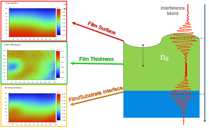
Figure 1. For each coating interface, fringes are formed at the top of the film and film/substrate interfaces as VSI scans down in measurement. Image Credit: Bruker Nano Surfaces and Metrology
Through-Film Thickness Measurements
Measuring the thickness of semi-transparent films can also be conducted via assessment of the film on the substrate, providing meaningful measurements of the film anywhere on the sample. Interferometric goals used in WLI measurements develop the moiré fringe envelope when put through focus.
Using a specialized Vertical Scanning Interferometry (VSI) mode, the interferometric objective moves vertically, allowing both the upper and lower surfaces of the film to come into focus as the scan progresses. This causes an interference fringe envelope pattern on each of the coating surfaces.
For each of the scan locations within the field of view, there are two sets of interference fringes for each of the camera pixels as the objective moves down. One of these objectives corresponds to the best focus at the top of the film, while the other corresponds to the film/substrate interface, as demonstrated in Figure 1.
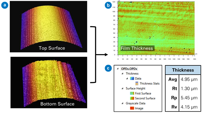
Figure 2. Cylindrical thick film analysis process: (a) top and bottom surfaces are measured, then (b) the cylindrical form is removed, and thickness is calculated with (c) the analysis tree to obtain thickness and surface finish metric outputs. Image Credit: Bruker Nano Surfaces and Metrology
Choice of objective lens influences measurable film thickness, due to both light penetration and fringe envelope separation. Lower magnification goals have a lower numerical aperture (NA). This means that more vertical light can enter the film, penetrating deeper, which enables measurement of thicker films.
For thin films, objectives with 50x magnification or higher have a shallower depth of focus but a higher numerical aperture (NA). This combination allows them to resolve the small spacing between two sets of interference fringes in films thinner than 2.0 μm. For the thinnest films, the fringe patterns tend to overlap regardless of the objective used. Due to this, a dedicated thin film analysis method, outlined in the next section, is necessary.
Transparent Films ≥2 μm (Thick Films)
Thick Film Analysis, a Vision64 software option, calculates thickness according to the fringes and separation of fringe envelopes. To begin, the analysis calculates the vertical center of each fringe envelope. It then determines the distance between the centers of each camera pixel. This distance is then divided by the film’s index of refraction to calculate thickness, as demonstrated in Figure 3a.
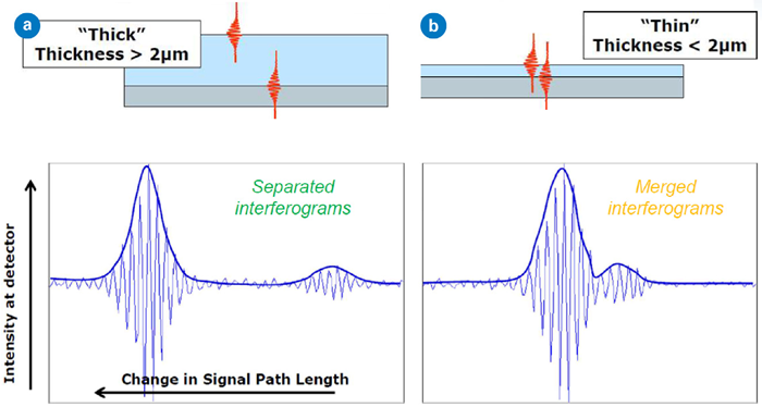
Figure 3. Fringe envelope using Thick Film Analysis for (a) >2 μm, where the envelopes are separated, and (b) <2 μm films, where the envelopes overlap and merge together. Image Credit: Bruker Nano Surfaces and Metrology
Table 1. Repeatability for semi-transparent films using various objectives measured by the Thick Film Analysis. Source: Bruker Nano Surfaces and Metrology
| Thickness (nm) |
Objective |
Std Dev (nm) |
Error (%) |
| 3283 |
50x |
1.2 |
0.04 |
| 11726 |
50x |
8.7 |
0.07 |
| 16044 |
20x |
13.8 |
0.09 |
| 2654 |
5x |
13.0 |
0.05 |
For the analysis to calculate thickness in a precise manner, the film’s index of refraction should be known, homogeneous, and typically assessed independently by reflectometry. If the index is unknown, the step measurement approach from the film surface to the substrate is utilized, and the index of refraction can be back-calculated and entered later.
Transparent Films <2 μm (Thin Films)
The thin film measurement mode was built for films with thicknesses under around 2 μm, where the fringe envelopes are practically merged together (as in Figure 3b), making it difficult to distinguish between them. Thin Film is a fringe-signal modelling algorithm that uses a merit function, which assesses agreement from the measured data and a built fitting model.
The fitting model, as demonstrated in Figure 4, is generated from a measurement model using the bare substrate after choosing magnification, together with the film and material calibration models available with Vision64 for several widespread film and substrate materials.
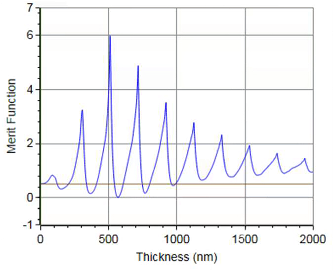
Figure 4. Example of a 600 nm thin film merit function model. Image Credit: Bruker Nano Surfaces and Metrology
In cases when a film model is not provided, custom models can be built by generating a table complete with different n and k optical values for the wavelengths covered for the new coating material.
When proper thin film models are generated for the materials to be assessed, Vision64 can automatically evaluate and calculate the film thickness within predefined boundaries, exhibiting a strong correlation with calibrated thicknesses, as demonstrated in Table 2.
Table 2. Thin film measurement table for correlation of certified thicknesses measured from 400-1100 nm for SiO2 film on Si. Source: Bruker Nano Surfaces and Metrology
|
Nominal (nm) |
Measured (nm) |
Error (%) |
| 1 |
394 |
365 |
-7.4 |
| 2 |
499 |
498 |
-0.2 |
| 3 |
632 |
611 |
-3.3 |
| 4 |
731 |
721 |
-1.4 |
| 5 |
829 |
821 |
-1.0 |
| 6 |
929 |
925 |
-0.4 |
| 7 |
1023 |
1020 |
-0.3 |
| 8 |
1123 |
1120 |
-0.3 |
Benefits of WLI for Film Thickness Metrology
WLI may be used to assess a broad range of film types and thicknesses, with either the step approach or through-film measurements, and has many considerable advantages:
- With through-film measurements, WLI assesses film thickness for every camera pixel in the field of view, underscoring thickness and uniformity variations over an area up to 15 mm in a single, quick measurement.
- The topography of the film and substrate surfaces is generated, giving a comprehensive view of coating uniformity and surface textures alike.
- A white-light interferometer’s range extends to tens of micrometers via the thick film mode and 10 mm using the step measurement approach.
- Optical profiling can be used to characterize surfaces that many other approaches cannot reach. These include the inside of coated cylinders as well as the bottom of narrow trenches.
- As WLI does not require any sample preparation, the approach enables non-contact, non-destructive analysis with feedback that is both immediate and fast.

This information has been sourced, reviewed, and adapted from materials provided by Bruker Nano Surfaces and Metrology.
For more information on this source, please visit Bruker Nano Surfaces and Metrology.