Two key steps are essential in semiconductor research, production, and quality control: first, verifying uniform crystal orientation in silicon wafers—crucial for achieving the desired electronic properties; and second, evaluating stress in thin films and integrated circuits, since stress resistance plays a major role in the performance, reliability, and lifespan of the final electronic device.
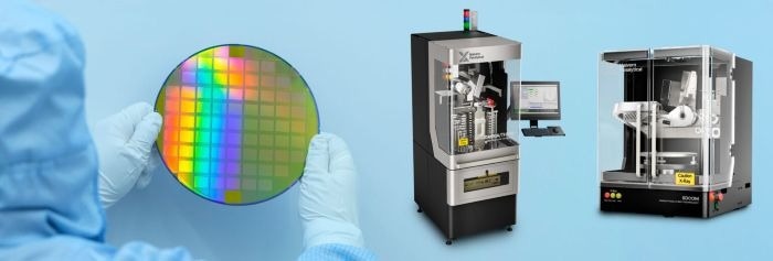
Image Credit: Malvern Panalytical
Although crystal orientation and stress mapping are critical across the industry, users have varying requirements when it comes to measurement speed, accuracy, and instrument footprint.
In this article, we compare Malvern Panalytical’s Omega/Theta and SDCOM systems—read on to learn which applications each system is best suited for.
What Determines Your Needs in Terms of Crystal Orientation and Mapping?
The ideal instrument would deliver top-tier accuracy at ultra-fast speeds, offer the flexibility to handle various sample sizes and analysis types and come in a compact format suitable for space-constrained environments.
However, in practice, a trade-off between these features is often necessary—so how do you determine the right balance for your needs?
You should consider:
- Precision: Do you need to detect ultra-fine stress gradients or misorientations, or just check basic crystal orientation?
- Flexibility: Do you require basic measurements or more extensive mapping and scanning capabilities?
- Are you studying small, experimental samples or large, standardized production samples?
- Cost efficiency: Are greater insights necessary, justifying a higher cost?
- For lengthier tests, ensure your equipment has cooling capabilities to avoid overheating.
Omega/Theta: A High-Precision Powerhouse
This system is designed for users who demand the highest levels of precision and flexibility. Applications such as evaluating residual stress in advanced nanoscale semiconductor devices or strained silicon channels benefit from the Omega/Theta’s exceptional 0.003° standard deviation, ensuring even the smallest misorientations or strain gradients are accurately detected.
The Omega/Theta also supports large-area mapping and can accommodate larger, heavier samples than the SDCOM. Its advanced functionality, such as Theta Scan and Rocking Curves, makes it well-suited for complex analytical tasks, offering detailed insights into stress distribution across intricate structures.
When this level of precision is required, researchers often extend data acquisition times to gain a more comprehensive understanding of their samples. Extended uptime can risk overheating, which is why the Omega/Theta is equipped with a water cooling system to maintain optimal performance during long-duration experiments.
With more orientation and transfer accessories than the SDCOM, and compatibility with advanced stacking and grinding stages, the Omega/Theta is a strong choice for researchers performing detailed, high-resolution material characterization.
SDCOM: The Compact and Efficient Solution
Not all applications require 0.003° standard deviation, advanced functionalities, or water cooling. For more basic and cost-effective crystal orientation measurements, SDCOM is the answer.
If your needs are for quality control in mid-scale integrated circuit fabrication, for instance, the larger operating area and more complex setup of the Omega/Theta would add unnecessary complexity without providing additional value.
Instead, the SDCOM’s compact benchtop design enables seamless integration into your workflows, and its faster setup makes it ideal for high-throughput environments. The SDCOM’s air-cooled system is also more cost-effective than its water-cooled counterpart, resulting in a low cost of operation and maximum profitability.
Yet, the SDCOM remains a powerful instrument: with an accuracy of up to 0.01° standard deviation, it can provide consistent and dependable results for most routine applications. It is also ideal for small-area mapping and can support stacking stages—although it remains best suited for less complex material analysis scenarios.
The SDCOM is, therefore, ideal when your crystal orientation and mapping needs are more basic or when a compact and cost-effective solution is needed for small samples and simpler setups.
Find the Best Solution for Your Needs
The flexibility of Malvern Panalytical’s portfolio for the semiconductor industry goes well beyond the Omega/Theta and SDCOM systems.
Whether you're focused on precision, speed, scalability, or cost-efficiency, the team at Malvern can help you identify the instrument that best fits your specific needs, challenges, and resources—and support you in unlocking new possibilities in material analysis.
SDCOM Demo at your desk
Video Credit: Malvern Panalytical
Omega/Theta Demo at your desk
Video Credit: Malvern Panalytical
Acknowledgments
Produced from materials originally authored by Jürgen Alizoti of Malvern Panalytical.
This information has been sourced, reviewed and adapted from materials provided by Malvern Panalytical.
For more information on this source, please visit Malvern Panalytical.