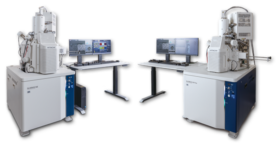
Hitachi High-Tech has recently introduced the SU3800SE and SU3900SE scanning electron microscopes (SEMs), which enhance the capabilities of the field-proven SU3800 and SU3900 models.

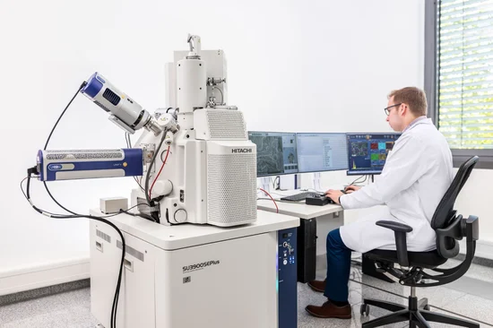
Image Credit: Hitachi High-Tech Europe
These new instruments are designed to meet specific application needs, offering two specimen chamber sizes and a choice between a thermal tungsten and Schottky field emitter.
The advanced Field Emission Optics instruments are set to significantly advance scientific research and industrial applications. Emphasizing productivity, the SU3800SE and SU3900SE automate critical optics alignment and repetitive operational tasks, enabling users to achieve reproducible results efficiently with minimal manual intervention.
As the demand for high-resolution imaging continues to rise across various sectors - including nanotechnology and industrial quality control - these new models empower researchers and manufacturers to gain deeper insights and enhancements in material analysis.
With these advancements, Hitachi High-Tech is committed to facilitating groundbreaking discoveries and improving product quality across multiple domains.

Image Credit: Hitachi High-Tech Europe
Need for Advanced Microscopy
Scanning electron microscopy has become essential in materials research and production control. This technique allows for high-resolution imaging of surface topography and composition of bulk or particle/filter samples.
However, the increasing demand for advanced microscopy techniques necessitates more sophisticated instruments that accommodate larger and heavier specimens while maintaining exceptional image quality and user-friendliness.
Many existing SEMs face limitations in handling large, heavy samples, often requiring additional specimen preparation, such as cutting, which is neither desirable nor feasible.
Furthermore, the growing application of SEMs for controlling microstructures to enhance material functionality and performance, as well as for analyzing foreign matter, faults, and defects to improve product quality, underscores the need for more versatile tools.
Integrating energy dispersive X-ray spectroscopy (EDS) and electron backscatter diffraction (EBSD) enables users to conduct comprehensive material analyses, from elemental composition mapping with EDS to crystallographic orientation studies with EBSD.
The increasing demand for these capabilities highlights the need for SEMs to efficiently manage complex, large-scale industrial specimens, such as vehicle components, while delivering high-resolution imaging and reliable data acquisition.
Benefits of the SU3800SE and SU3900SE
The SU3800SE and SU3900SE SEMs from Hitachi High-Tech address these challenges with various features and benefits designed to enhance user experience.
Large, Heavy and Multi-Specimen Handling Ability
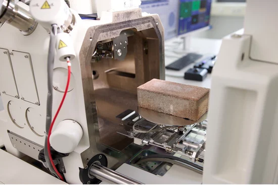
OA's key feature of the SU3800SE, particularly the SU3900SE, is their ability to accommodate larger bulk samples on their 5-axis eccentric specimen stages. With all five stage axes available, the SU3900SE can handle specimens up to 300 mm in diameter, 130 mm in height, and 5 kg in weight.
This capability reduces or eliminates the need to cut larger test items, enhancing productivity by allowing the loading of multiple specimens for sequential analysis.

Samples up to 300 mm diameter can be fully inspected (SU3900SE). Image Credit: Hitachi High-Tech Europe
Effortless and Safe Sample Navigation
These new SEMs also incorporate an advanced optical camera navigation system that encompasses the entire range of X,Y stage motion, facilitating easy location and access to specific specimen positions with a simple mouse click.
The optical camera follows the stage rotation, providing a seamless sample navigation experience - ideal for users engaged in complex and detailed analyses.
Another noteworthy feature is the automatically applied sample and stage collision model, ensuring that any available stage motion poses no risk. This allows users to fully leverage the SEM’s capabilities; for instance, the shortest working distance for the highest resolution can be set without hesitation.
Optimal System Performance
The SU3800SE and SU3900SE are equipped with fast, modular, reliable, and precise automated functions for electron optics alignment, focusing, anti-stigmation, and brightness/contrast adjustments.
Coupled with a user-definable library of observation condition recipes, these features empower users of varying expertise to consistently produce high-quality images, leveraging advanced electron optics and detection technology.
EM Flow Creator
Routine inspection tasks should not constrain operators to the SEM. The SU3800SE and SU3900SE offer the optional EM Flow Creator function, which facilitates the configuration of complex workflows without the need for programming or coding skills.
EM Flow Creator achieves this by arranging graphically defined function blocks - such as magnification, stage position, and image adjustment functions like focus and contrast - alongside decision-making events, repeating loops, and pattern matching. Once established, these workflows can be executed automatically, thereby reducing workload and ensuring consistent, high-quality results.
These advantages allow you to concentrate on your research while the microscope manages intricate tasks. These SEMs automate processes and guarantee accurate, high-quality outcomes with minimal manual intervention.
Applications and Impact
The introduction of Hitachi's SU3800SE and SU3900SE signifies a significant advancement in microscopy technology, with extensive applications across multiple disciplines.
Nanotechnology
In nanotechnology, where precision at the nanoscale is critical, these new SEMs enable researchers to observe and analyze nanostructures with exceptional detail.
The high-resolution imaging capabilities facilitate the characterization of nanomaterials, empowering scientists to investigate their unique properties and potential applications in electronics, medicine, and materials science.
Industrial Quality Control
These advanced SEMs allow manufacturers to perform comprehensive inspections of materials and components for industrial applications, particularly in quality control. By identifying defects and analyzing microstructures, companies can enhance product quality and performance, reduce waste, and improve efficiency.
The SU3800SE and SU3900SE's design accommodates larger specimens and delivers high-quality imaging of conductive and, through the standard-provided variable chamber pressure mode, non-conductive samples.
This enables a thorough analysis of industrial materials, such as metals, composites, and vehicle parts, without requiring additional processing.
Materials Science
In materials science, the new models support critical research to understand the properties and behaviors of various materials.
Their enhanced imaging capabilities allow for the examination of surface topography and composition, providing insights that drive innovation in material development.
This is particularly crucial for advancing cutting-edge materials in aerospace, automotive, and electronics industries, where performance and reliability are paramount.

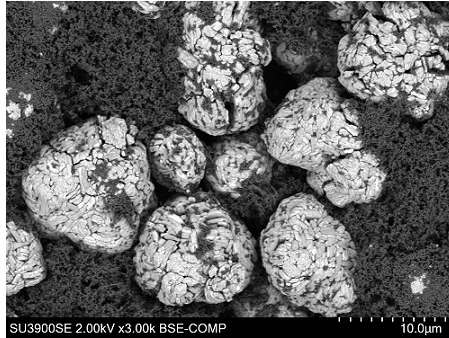
LiB cathode material - Distributions of cathode material particles and surrounding binder can be seen. Image Credit: Hitachi High-Tech Europe
Conclusions
Hitachi's SU3800SE and SU3900SE scanning electron microscopes represent a significant advancement in microscopy.
With their capability to accommodate larger specimens, advanced automation features, and user-friendly design, these SEMs are poised to become indispensable tools for both industrial and academic users.
They enhance the efficiency and accuracy of microscopy while future-proofing laboratories by offering the adaptability required to meet evolving research and production demands.

This information has been sourced, reviewed and adapted from materials provided by Hitachi High-Tech Europe.
For more information on this source, please visit Hitachi High-Tech Europe.