In today's fast-changing technological landscape, two key theories determine the future of semiconductor design: Moore's Law and the More-than-Moore approach.
While Moore's Law focuses on increasing transistor performance and efficiency, the More-than-Moore approach explores functional diversity via heterogeneous integration.
Both approaches encourage the development of new packaging technologies, which are critical for driving innovation in areas such as high-performance computing, 5G, automotive, photonics, and artificial intelligence.
As semiconductor integration becomes more complicated, improved metrology techniques become crucial to assuring performance, dependability, and manufacturing precision.
Techniques Of Metrology in Advanced Packaging
Optical metrology is used throughout the process to ensure process accuracy, optimize performance, and minimize defects in next-generation semiconductor packaging.
One important criterion that distinguishes advanced semiconductor architecture is the depth of the interposer layer, which is meant to be as thin as possible to take up the least amount of space.
Sensofar's S neox profiler uses interferometry at low magnification to precisely quantify through-silicon-vias depths, even in ultra-thin interposers.
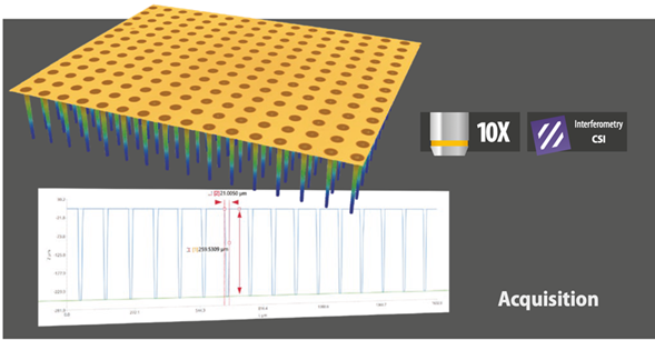
Figure 1. Through-silicon-vias, description: Topography of through-silicon vias (TSVs), showing depth characterization across the array. Image Credit: Sensofar Metrology
Another critical aspect of semiconductor design is microbumps, vital in 2.5D and 3D integration as they provide electrical and mechanical connections between stacked dies or interposers. Sensofar's SensoPRO Bump Analysis plugin automates bump height and coplanarity adjustment, helping to eliminate bonding failures and ensure electrical dependability.
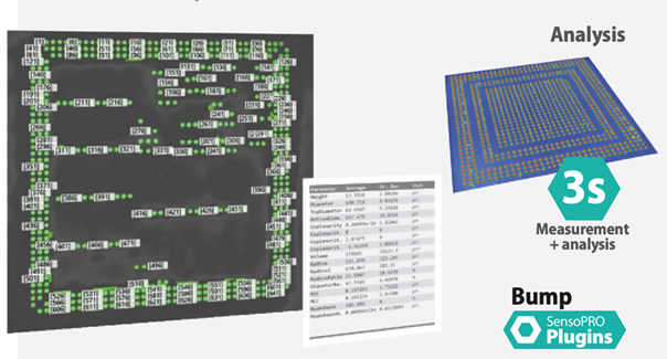
Figure 2. Microbumps, description: Topography of microbumps, illustrates coplanarity and height distribution. Image Credit: Sensofar Metrology
Wafer glue uses these sticky layers to secure dies or wafers during processing. Sensofar's Wafer Glue and Glue Height plugins can automatically characterize adhesive thickness and homogeneity, ensuring consistent adhesion and mechanical stability.
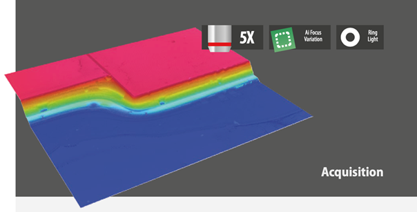
Figure 3. Wafer Glue, description: Topography of an adhesive layer in wafer bonding. Image Credit: Sensofar Metrology
Redistribution layers are key components that provide electrical connections between the die and external circuitry, ensuring the precision of the traces.
Figure 4. FOPLP, description: Topography of redistribution layers (RDLS) in Fan-Out Panel-Level Packaging (FOPLP). Image Credit: Sensofar Metrology
Advanced packaging uses wafer-level processing, including typical semiconductor manufacturing methods such as Front-end-of-Line (FEOL) and Back-end-of-Line (BEOL).
At this stage, bump inspection, die attachment, wafer cutting characterization, and CMP pad characterization are required to ensure exact interconnect creation, defect-free surfaces, and mechanical integrity for heterogeneous integration.
These processes are effectively implemented using Sensofar's instruments, including hardware (profilometers S neox and S lynx) and software (SensoPRO plugins). These connections provide comprehensive automation and reproducibility.
More information about these solutions and industrial use cases can be found on Sensofar's Advanced Packaging applications website.
How Does Heterogeneous Integration Improve Our Technologies?
Heterogeneous integration is critical for all applications that demand fast data transport, energy-efficient computation, and complicated multifunctional integration. In addition, heterogeneous integration extends to multi-chiplet systems, in which specialized processors, memory, and accelerators are combined into a single package.
Like advanced packaging, as all these technologies continue to evolve, high-precision 3D optical metrology aims to ensure exact alignments, surface quality, and bonding integrity across varied materials and components, fostering innovation in next-generation semiconductor packaging.
Microlenses are one of the components for which metrology has a special issue. They provide a variety of functionalities that would be impossible to execute with conventional components.
Microlenses have spherical and aspherical geometries, and so require strict metrology accuracy regarding resolution and surface smoothness.
Sensofar delivers sub-nanometer precision using PSI and ePSI modes, and the SensoPRO Aspherical and Spherical plugins automatically extract metrics like radius, height, and residual roughness.
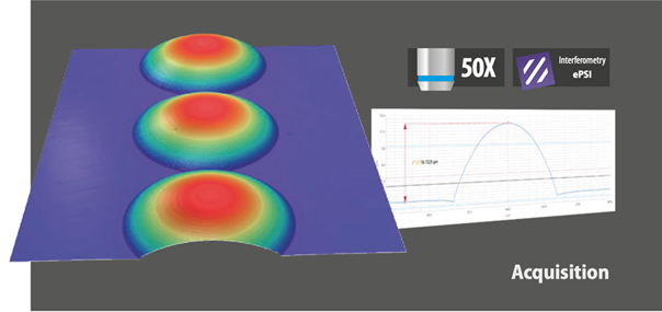
Figure 5. Microlenses, description: Topography of microlenses, showing curvature and surface quality parameters. Image Credit: Sensofar Metrology
Micro-Electromechanical Systems (MEMS) are also important components in heterogeneous integration because they allow the seamless mixing of mechanical, optical, and electronic functionalities into a single package.
Sensofar's confocal, interferometry, and focus variation techniques enable precise profiling of MEMS microstructures, curvature analysis, and surface integrity testing.
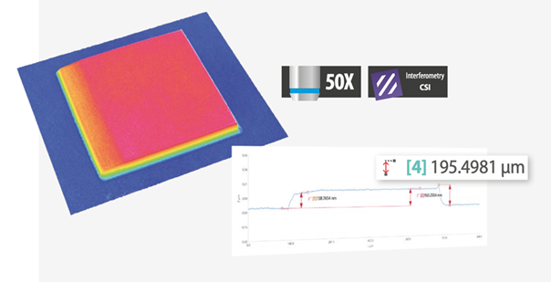
Figure 6. MEMS, description: Topography of Micro-Electro-Mechanical Systems (MEMS), the key component in heterogeneous integration. Image Credit: Sensofar Metrology
Printed Circuit Boards (PCBs) play an important role in these phases. They act as the basic interconnect platform, allowing communication between various semiconductor components.
Sensofar's non-contact optical metrology maintains the quality of interconnects, surface uniformity, and structural reliability in high-density printed circuit boards.
By combining multiple materials and technologies, heterogeneous integration and advanced packaging are driving semiconductors towards greater efficiency and more compact designs.
Overall, Sensofar's 3D optical profilometers play a key role in the future of semiconductor production with their accuracy, repeatability, and automation, which are required to meet the severe criteria of advanced packaging and heterogeneous integration.

This information has been sourced, reviewed, and adapted from materials provided by Sensofar.
For more information on this source, please visit Sensofar Metrology.