Many of today’s technological advances center around semiconductors. They contribute to almost all of their utilities as well as real performance. To produce the powerful tech, a number of manufacturing steps are required, and most of them rely heavily on metrology. But why and how does metrology affect semiconductor fabrication?
Silicon: The Most Widely Used Material in Semiconductors
With its superb electrical characteristics, silicon is at the heart of most semiconductors. Its ability to control electrical characteristics has made it essential in modern electronics.
Three distinct steps must be applied to raw silicon before it becomes a fully working chip, all of which require high-quality materials and excellent performance. The first stage is to turn silicon into thin wafers of semiconductor material. These layers are necessary to manufacture semiconductor devices.
Each wafer must meet high purity, flatness, and cleanliness standards to ensure optimal performance in later manufacturing phases. Sensofar uses PSI interferometry to evaluate sub-nanometer roughness on bare wafers, guaranteeing they are defect-free and ready for front-end processing.
Research introducing new semiconductor materials such as SiC, GaN, diamond, or perovskites can pose even greater hurdles, requiring precise control over surface quality and thickness.
Sensofar's solutions are already being used to test these wafers, including vacuum rings in wafer loaders, where flatness is required to avoid breakage.
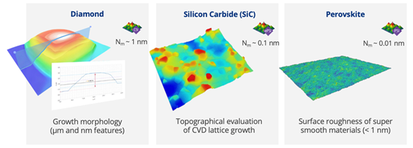
Figure 1. Image Credit: Sensofar Metrology
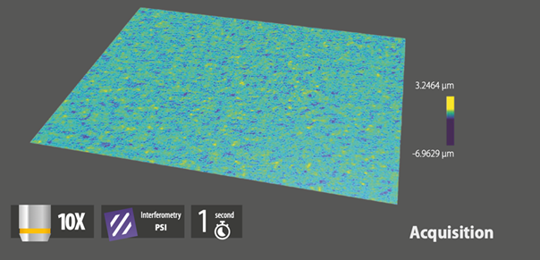
Figure 2. Perovskites, description: Surface roughness of perovskites is closely linked to the manufacturing quality. Image Credit: Sensofar Metrology
Silicon ingots, large blocks of silicon, are the primary material used in semiconductor manufacturing. They are created by melting high-purity silicon and gradually cooling it to form a single crystal structure. Once formed, the ingot is sliced into the thin wafers used to manufacture computer chips and other electrical devices.
The second stage, front-end processing, involves placing the primary structures of an integrated circuit on a silicon wafer. All of the operations involved in these steps are repeated numerous times in different sequences to create the multi-layered architecture of a semiconductor device, using various materials and changes.
At this level, Sensofar's systems manage thin-film thickness, analyze EUV photomasks, evaluate etching depth and sidewall profiles, and even monitor CMP pad wear in real time with the S mart 2 sensor. These measurements help maximize yield and ensure dimensional accuracy at every stage.
Interferometry and spectroscopic reflectometry are used to evaluate thin oxide layers on the nanometer scale.
Similarly, EUV masks are assessed at nanoscale precision to ensure pattern fidelity during lithography. In planarization, pad life is increased through in situ monitoring of glazing and groove occlusion, which decreases consumables and improves process stability.
This starts with oxidation and deposition to create insulating and conductive layers on the wafer to prepare it for further patterning.
Once layered with insulation and conduction materials, the wafer is coated with a photoresist substance, which allows for exact pattern transfer. During lithography, ultraviolet light imprints the complicated semiconductor design onto the wafer, establishing the circuit's layout.
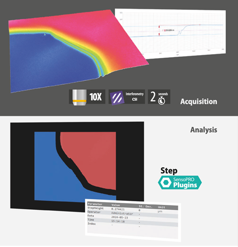
Figure 3. Film thickness, description: Thin film thickness measurement. S neox can accurately measure film thickness using Spectroscopic Reflectometry and Interferometry techniques. Image Credit: Sensofar Metrology
Following imprint, etching selectively removes undesired material from circuit architectures, followed by doping and ion implantation, which add controlled impurities to affect the electrical properties of distinct regions.
Finally, planarization creates a flat, uniform surface by removing superfluous material, allowing for the precise stacking of subsequent layers.
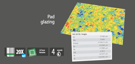
Figure 4. Pad glazing, description: Topography of Chemical Mechanical Planarization (CMP) with ISO 25178 roughness parameters. Image Credit: Sensofar Metrology
The third phase, back-end processing, includes breaking the wafer into individual dies, allowing for reliable electrical connections and desired performance. This final stage focuses on interconnecting, packing, and testing individual chips to ensure proper functionality.
During this step, Sensofar's optical profilers check dicing accuracy, analyze die-attach adhesives, measure bump coplanarity, and inspect encapsulation aspects like pin flatness and marking depth to guarantee final devices fulfill reliability standards.
In wafer dicing, plugins like Cross Kerf can be used to confirm the depth and uniformity of the cuts. During bonding, adhesive layers are evaluated for homogeneity, flip-chip bumps are inspected for coplanarity, and wire bonding is certified by automatically verifying intermetallic coverage.
In encapsulation, Fringe Projection assures pin coplanarity and laser marking depth, while final testing involves inspection of probe marks and bumps following electrical validation.
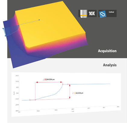
Figure 5. Die adhesion, description: Topography of a die-attach adhesive layer, highlighting thickness and spread uniformity for reliable semiconductor bonding. Image Credit: Sensofar Metrology
The first step, wafer dicing, entails cutting the processed wafer into individual dies that may be connected electrically. The next stage, encapsulation, protects the chips from external influences, including dust and moisture.
Final testing completes the process, involving a variety of tests that validate properties such as the conductivity of the chip's connecting points, assuring correct functionality before integration into electronic equipment.
Future Trends in Semiconductor Manufacturing
The semiconductor industry is characterized by its complexity and innovation, and key to this is its precision and strict process control for high-quality results.
Each aspect of wafer manufacturing, testing, and packaging must comply with rigorous standards to maintain high yields and reliability in advanced applications.
Sensofar's 3D optical metrology systems are already being used at these stages, from wafer surface preparation to package inspection, as seen on the company’s semiconductor applications website.
Metrology is critical to this process since it helps with quality control, yield optimization, and overall manufacturing efficiency.
As the industry pushes toward advanced packaging solutions, new levels of performance, energy efficiency, and functionality emerge, all while allowing for further downsizing.
These developments are especially important for technologies like artificial intelligence, high-performance computing, and the Internet of Things (IoT).
To keep up with this progress, metrology must also evolve, providing precise measuring capabilities at both the wafer and packaging levels to maintain manufacturing standards and ensure long-term device dependability.

This information has been sourced, reviewed, and adapted from materials provided by Sensofar.
For more information on this source, please visit Sensofar Metrology.