By adjusting the atomic precursor pulses, researchers demonstrated that 2D semiconductor alloys can be built with controlled composition, embedded nanoscale structures, and tunable light-emitting behavior.
Study: Control of composition and atomic distribution in ternary molybdenum tungsten disulfide monolayers by sub-atomic layer deposition
The development of advanced electronics has heightened interest in two-dimensional (2D) transition-metal dichalcogenides (TMDs) due to their unique properties. A recent study published in npj 2D Materials and Applications demonstrates controlled composition and atomic distribution in ternary molybdenum-tungsten-disulfide monolayers via sub-atomic layer deposition (sub-ALD). This allows the fabrication of monolayer alloys across the full compositional range, enabling fine control of the material’s local electronic structure, which is crucial for advanced electronic and optoelectronic devices.
Advancements in TMD Alloying Techniques
In recent years, TMDs have emerged as key materials for next-generation electronics because they exhibit direct band gaps when reduced to a single-layer thickness. Alloying different transition metals within a single crystal lattice allows continuous tuning of electronic properties, particularly the bandgap, enabling customization for specific applications.
Conventional synthesis methods, such as chemical vapor deposition, have been used to grow these alloys, but precise control over metal-atom distribution remains important for reproducible material properties. Therefore, there is a need for innovative fabrication methods that achieve accurate atomic-level control over material composition and structure.
Methodology for Enhanced Material Growth
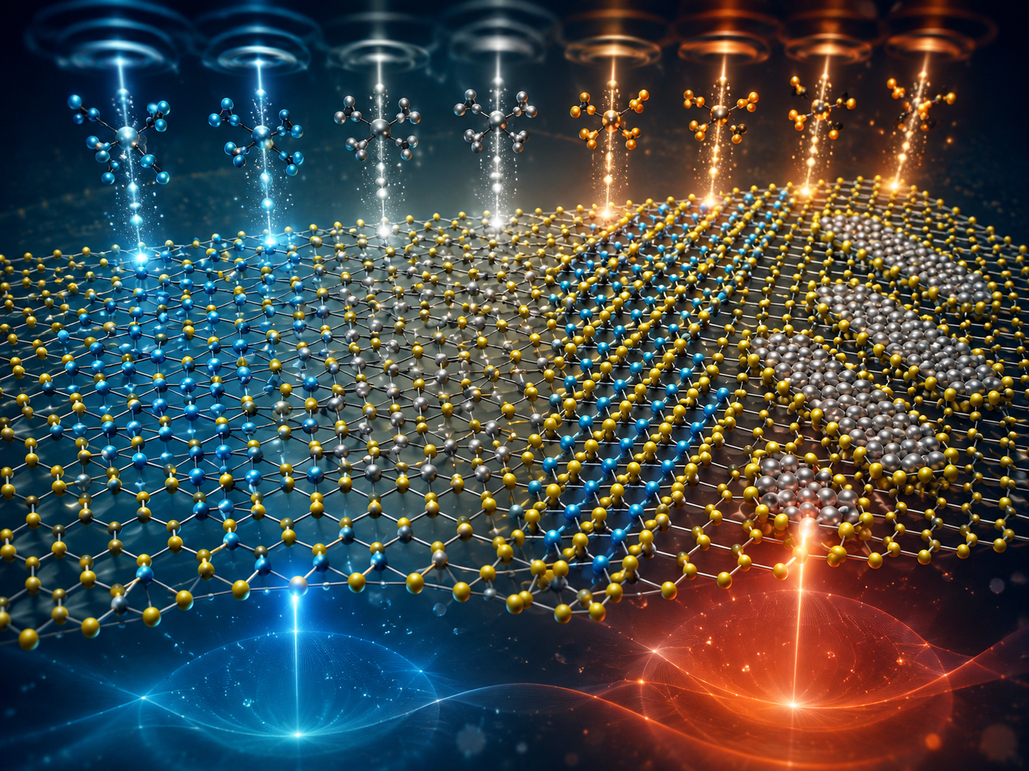
To address these limitations, researchers in Germany developed a modified atomic layer deposition method to control material growth at the sub-atomic-layer level. Instead of relying on random mixing of molybdenum and tungsten atoms during deposition, this approach uses carefully timed precursor pulses to control their incorporation into the monolayer. By adjusting the deposition sequence, the authors achieved both homogeneous alloys and intentionally inhomogeneous nanostructures, such as line patterns and elongated islands, enabling precise composition engineering at the atomic scale.
The resulting structures were verified using high-angle annular dark-field scanning transmission electron microscopy (HAADF-STEM), which provided atomic-resolution images of metal atoms within the monolayer lattice and confirmed the controlled incorporation of molybdenum and tungsten atoms. However, STEM imaging also showed bilayer, multilayer, and amorphous regions alongside monolayer areas, indicating that the ALD process still requires optimization to achieve monolayer-only growth. Raman spectroscopy tracked shifts in the characteristic A1′ phonon mode, allowing for estimation of the molybdenum-tungsten alloy composition. Photoluminescence spectroscopy was used to examine how variations in atomic distribution influenced excitonic emissions and emission energies.
Excitonic Behavior in Engineered Monolayers
The alloy composition was continuously tuned across the full molybdenum-tungsten range by adjusting the precursor pulse sequence. This process produced two distinct atomic configurations: homogeneous random alloys and intentionally inhomogeneous nanostructures containing line patterns and elongated islands. Such structural control provides a powerful means of tailoring the electronic properties of monolayer materials.
Optical measurements showed significant changes in the A and B excitonic transitions. In homogeneous alloys, the excitonic energies exhibited bowing behavior, reflecting the nonlinear evolution of the bandgap between the two parent compounds, with bowing parameters of 0.216 eV for the A exciton and 0.023 eV for the B exciton. In contrast, nanostructured monolayers displayed clear deviations from this trend. These differences were linked to changes in the electronic energy landscape, where atomic line features and islands created local energy minima that can trap electrons and shift excitonic recombination energies.
Implications for Advanced Device Fabrication
The ability to precisely engineer ternary TMD monolayers opens new opportunities for advanced research on electronic and optoelectronic materials. Using subatomic-layer deposition, researchers can fabricate continuous monolayers containing embedded MoS2- or WS2-rich nanoscale regions, thereby offering a potential route to engineered 2D heterostructures rather than demonstrating finished devices.
These atomically customized materials are promising for future excitonic and nanoscale optoelectronic research, although the study did not fabricate or test device performance. In particular, localized energy wells associated with nanoscale island structures may support future attempts to form quantum-dot- or quantum-wire-like regions within 2D TMD layers. Control over composition and atomic arrangement can also be used to study charge localization and carrier confinement, supporting the development of future nanoscale device architectures.
Future Prospects in Quantum Material Engineering
In summary, this study marks a step toward deliberate atomic-scale engineering. The implementation of sub-atomic layer deposition shows that chemical composition and atomic arrangement can be controlled within a single fabrication process, addressing a key challenge in the controlled growth of complex 2D materials.
The approach also provides a practical framework for designing possible quantum-confined structures directly within monolayer materials. Further refinement of precursor pulse sequences could enable future attempts to fabricate quantum wires, quantum dots, and other nanoscale architectures with tailored electronic and optical properties. Overall, such capabilities could play a key role in the development of future quantum materials and devices.
Download your PDF copy by clicking here.
Disclaimer: The views expressed here are those of the author expressed in their private capacity and do not necessarily represent the views of AZoM.com Limited T/A AZoNetwork the owner and operator of this website. This disclaimer forms part of the Terms and conditions of use of this website.
Source:
- Tessarek, C., et al. (2026). Control of composition and atomic distribution in ternary molybdenum tungsten disulfide monolayers by sub-atomic layer deposition. npj 2D Materials and Applications. DOI: 10.1038/s41699-026-00710-4. https://www.nature.com/articles/s41699-026-00710-4