Fluorescence Lifetime Imaging Microscopy (FLIM) is used to determine the photoluminescent (PL) properties of LED materials.1
- FLIM Microscopy maps photoluminescence lifespan in LED structures with spatial resolution.
- Defects caused by sidewall damage can affect LED performance and recombination efficiency over time.
- The MicroPL allows for simple FLIM measurements and high-resolution mapping of III/V semiconductor LED chips.
Studying III/V Semiconductors with FLIM
FLIM investigates excited-state dynamics and local environments by mapping PL lifetimes over a sample. This information is critical for understanding and enhancing LED efficiency and stability.
Defects in III-V semiconductors can degrade LED performance by lowering radiative recombination efficiency. FLIM allows you to directly visualize this impact and generate measures to reduce defect-related losses.
III-V semiconductors, such as AlInGaP and GaAs alloys, are particularly appealing for LEDs due to their tunable direct band gaps (Figure 1).
These materials enable visible emission profiles while providing greater thermal stability and device efficiency than II-VI or indirect-bandgap semiconductors such as silicon or silicon carbide. AlInGaP/GaAs LED chips, for example, are frequently used for intense red, orange, and yellow light emissions.
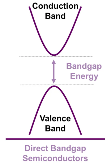
Figure 1. Direct bandgap of III/V-semiconductors illustrating the tuneability of emission wavelength in LED materials. Image Credit: Edinburgh Instruments
With such high-performance materials, comprehensive characterization technologies are key to fully realizing their potential.
This article shows how to perform FLIM using the Edinburgh Instruments MicroPL update, compatible with the FS5 and FLS1000 PL spectrometers (Figure 2). The technique is used to investigate the emission properties of LEDs, which can aid in chip design optimization and knowledge of performance constraints.
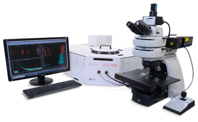
Figure 2. MicroPL coupled to an FLS1000 PL Spectrometer for FLIM mapping. Image Credit: Edinburgh Instruments
Materials & Methods
AlInGaP/GaAs visible LED devices were used (Figure 3) to explore the PL properties of the epitaxial AlInGaP layer. This experiment investigated an orange LED emitting at 610 nm.
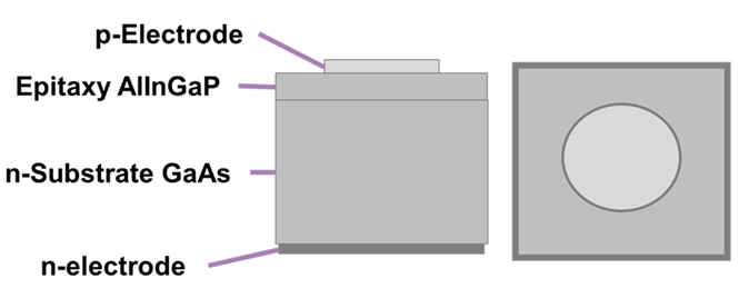
Figure 3. Structure of AlInGaP/GaAs LED Chip. Image Credit: Edinburgh Instruments
FLIM mapping was done with the MicroPL upgrade and a FLS1000 spectrometer outfitted with a 485 nm pulsed diode laser excitation source and a high-speed hybrid photodetector (HS-HPD).
Time-Correlated Single Photon Counting was used to measure PL lifetimes. Table 1 shows the full set of experimental parameters.
Table1. Experimental parameters of FLIM mapping. Source: Edinburgh Instruments
| Parameter |
Measurement |
| Excitation source |
HPL-485 |
| Acquisition mode |
TCSPC |
| Dichroic filter |
495 nm |
| Objective lens |
40x /0.75 |
| Emission wavelength |
610 nm |
| Map step size |
3 μm |
| Repetition rate |
5 MHz |
| Dwell time |
0.5 s |
| Detector |
HS-HPD |
FLIM Mapping of the LED Chip
FLIM mapping of the LED chip surface, comprising the p-electrode and epitaxial AlInGaP layer, revealed spatial differences in lifetime (Figure 4). The results showed that the AlInGaP layer had an average lifetime of approximately 5.5 ns.
The lifetime was observed to fall to roughly 2.5 ns at the LED chip's borders. In addition, no PL signal was detected at the chip’s p-electrode, as expected given that the electrode material absorbs excitation and PL light, limiting measurement of the underlying active layer.
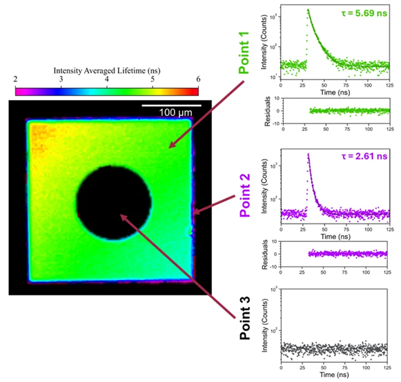
Figure 4. FLIM map of AlInGaP/GaAs LED chip showing variation in lifetime across the chip. The inset shows PL lifetime at three distinct points of the chip – Point 1: Epitaxy AlInGaP, Point 2: Edge of LED, and Point 3: p-electrode. Image Credit: Edinburgh Instruments
The shorter lifetime at the chip edge is due to the sidewall effect, which is performance degradation induced by plasma damage to the LED’s sidewall during the fabrication process.2
These sidewall flaws have a major impact on device performance, including carrier dynamics, light extraction efficiency, and epitaxial layer quality. Optimizing sidewall features like angle, smoothness, and etch quality is thus crucial for producing high-performance LEDs.
Conclusion
The researchers used FLIM with the MicroPL update for the FLS1000 to map the radiative recombination kinetics of AlInGaP/GaAs LEDs. This spatially resolved research indicated a significant reduction in carrier lifetime at the chip edges, which directly correlates with the sidewall effect.
These unique FLIM insights can be used to optimize manufacturing processes and chip design, ultimately enhancing LED efficiency and speeding up breakthroughs in solid-state lighting and display technologies.
References
- Lakowicz, J.R. (2006). Principles of Fluorescence Spectroscopy. Boston, MA: Springer US. DOI: 10.1007/978-0-387-46312-4. https://link.springer.com/book/10.1007/978-0-387-46312-4.
- Liu, Z., et al. (2025). Advanced technologies in InGaN micro-LED fabrication to mitigate the sidewall effect. Light: Science & Applications, 14(1). DOI: 10.1038/s41377-025-01751-y. https://www.nature.com/articles/s41377-025-01751-y.

This information has been sourced, reviewed, and adapted from materials provided by Edinburgh Instruments.
For more information on this source, please visit Edinburgh Instruments.