A central principle of materials science is the relationship between structure and properties, especially the way microstructure influences local mechanical performance. Understanding this link is important in a wide range of applications.
Traditionally, the process for collecting co-located data for a correlation analysis follows the steps: measure → transfer → locate → measure. The transfer phase relates to the pass between a microscope and a nanoindenter.
Yet workflow inefficiencies can introduce errors due to misalignment or sample damage during transfer. The PI 89 Auto SEM PicoIndenter® circumvents any restraints by facilitating direct, targeted nanoindentation in the scanning electron microscope (SEM) via a dual-axis rotation and tilt (R/T) stage.
Users can select features in an electron or EDS/EBSD image and then immediately indent at those same coordinates within a single unit. The results, a simple measure → measure workflow.
This article includes a case study discussing co-located imaging and nanomechanical data collection on laser-clad steel using PI 89 Auto™. The results demonstrate an effective, accelerated correlation between microstructure and mechanical properties.
Instrument Configuration and Workflow Overview
The Hysitron® PI 89 Auto SEM PicoIndenter is an in situ nanoindenter that seamlessly integrates into SEM workflows. PI 89 Auto includes a patented two-axis R/T stage that provides an additional 2 degrees of tolerance to the PI 89 base platform.
The extra degrees of freedom allow PI 89 Auto’s stage to be angled precisely for nanoindentation, EBSD, and top-down SEM imaging – together with secondary electron (SE), backscattered electron (BSE), and energy-dispersive X-ray spectroscopy (EDS) imaging. All of this is possible without removing the specimen from the chamber (Figure 1).
TriboScan™ software offers precise instrument control and directly transmits all information to Bruker ESPRIT™ EBSD systems. Users can indent locations in line with any imaging modality and move effortlessly to the indentation at the targeted position.
For both the SEM-column and the EBSD orientations, calibration should be conducted once per session to record the indentation and imaging coordinate systems. These two-orientation methods help ensure reliable targeting across all workflows.
Once calibration has been performed, users need only select the areas of interest from SE/BSE/EDS/EBSD images. Coordinates are then transmitted to TriboScan, which calculates and initiates the indentation workflow at the associated position. Targeting is as easy as a single click from the imaging modality interface.
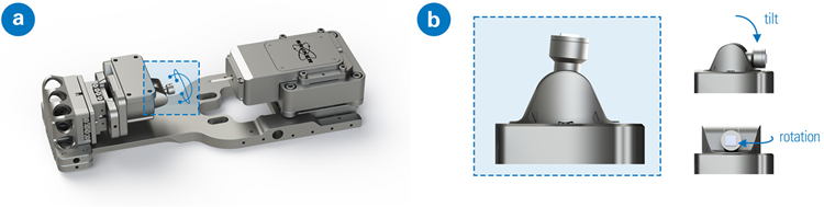
Figure 1. (a) PI 89 Auto system equipped with R/T stage and (b) illustration of the two axes of movement. From the indentation orientation (in the box), the stage can be tilted for SEM column access or rotated for EBSD access. Image Credit: Bruker Nano Surfaces and Metrology
Materials and Methods
As described by Haake and Zediker, a 4140-steel substrate was laser clad with 410 stainless steel powder.1 Preparation of a cross-section of the cladded material was carried out according to EBSD quality: ground up to 1200 grit with SiC metallographic paper, polished using diamond suspensions, and finished with 10 min of polishing using 50 nm colloidal alumina.
For this case study, the PI 89 Auto system was fitted with a 30 μm-range piezoelectric actuator, a 500 mN xR high-load transducer, and a diamond Berkovich probe. Indentation grids were conducted using Bruker’s XPM™ accelerated property mapping, executed by displacement control to a maximum depth of 150 nm and segment times of 0.1s for both loading and unloading.
One XPM map per region (410, heat-affected zone (HAZ), 4140) contained 25×25 indents over 75×75 μm2, with 3 μm indent spacing to limit interaction between adjacent indents.2
Prior to indentation, EBSD was used for scanning, then XPM map coordinates were determined via the EBSD view. Re-scanning of the same area was performed post-indentation to arrange indents in-line with microstructural features.
To ensure capture of all gradients across interfaces, a continuous line scan was taken from the 4140 region through into the 410 cladding. The line scan used the XPM load function to execute as a line of 825 indents over 2475 μm (3 μm/indent). 4140 bulk behavior was captured >1 mm from the HAZ (as determined by BSE imaging) prior to entering the transition region.
Results and Discussion
Microstructure Analysis
The cross-section images based on chemistry (EDS) and microstructure (concentric backscatter, CBS) are displayed in Figure 2 and reveal three distinct areas. There is clear CR abundance visible in the 410 cladding zone on the left, to the right, the base 4140 region presents distinct grain structure, and the central HAZ has lower Cr concentration and a distinct lack of clear microstructural features.
Taken from the Cr interface to the start of the base 4140 grain structure, the HAZ spans 650-800 μm.
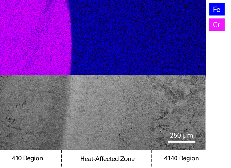
Figure 2. Composite micrograph composed of (top) EDS and (bottom) CBS images to show distinct zones based on Cr concentration and grain orientation. Image Credit: Bruker Nano Surfaces and Metrology
Targeted Hardness Mapping
Prior to indentation, an EBSD scan of the 410 cladding (Figure 3a) displayed a two-phase region with clusters of precipitates and large grains, both of which indexed as ferrite. It is presumed that the large grains are ferrite, whereas the clusters of precipitates are considered to be tempered martensite.
The post-indentation EBSD scan shows visible indents (Figure 3b) resulting from the high local deformation attributable to indentation. The grid itself shows distortions in Figure 3b due to the pre-tile adapter imposing a specific imaging angle, as clarified in the targeting calculations.
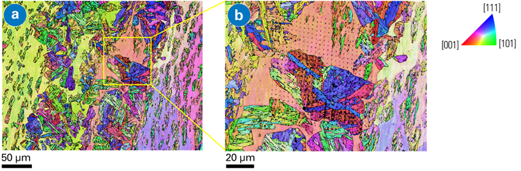
Figure 3. (a) Composite inverse pole figure (IPF) and band contrast (BC) map of pre-indentation EBSD scan in the 410 region, showing large ferritic grains and clusters of tempered martensite. (b) Post-indentation IPF/BC map from the marked area in (a), illustrating indentation targeting accuracy. Image Credit: Bruker Nano Surfaces and Metrology
With only 16 μm from the targeted position to the edge of the indentation area, targeting was precise. Figure 4a displays the same microstructure from Figure 3b aligned with the PI 89 axes via rotation, thus enabling direct comparison with the mechanical maps.
Reduced hardness in the large ferritic grains (blue, average 3.01 GPa) can be seen in the hardness map (Figure 4b), whereas the martensitic clusters have greater hardness (red, average 4.89 GPa). This contrast is mirrored in the reduced modulus map (Figure 4c), where higher modulus corresponds to the harder regions.
It should be emphasized that the rapid speeds of the indentation process can produce an increase in the material hardness observed in relation to quasistatic indentation, as a potential result of material strain rate sensitivity.2
All materials were examined under the same loading profile, enabling verifiable relative comparisons.
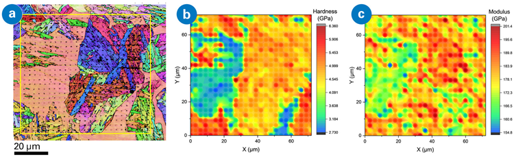
Figure 4. (a) IPF/BC microstructure from Figure 3 rotated to the PI 89 Auto coordinate system (yellow box outlines the indentation grid). (b) Hardness map showing higher hardness in the tempered martensite clusters and lower hardness in ferrite. (c) Reduced modulus map showing the same spatial contrast. Image Credit: Bruker Nano Surfaces and Metrology
Hardness Profiling Across Clad Interface
Results from the line of indents are displayed in Figure 5, parallel to those shown in Figure 2 (the 410 cladding on the left and 4140 region on the right).
Hardness from the line scan is approximately 3 GPa across the initial ~1 mm of the 4140 region. An increase in scatter and a rise in mean hardness are observed when approaching the HAZ; peaks are seen around 6 GPa near the Cr interface.
Average hardness decreases upon entering the 410 cladding, but bimodality is observed in the scatter, which is consistent with the dual-phase ferritic–martensitic microstructure. In Figure 5, box-and-whisker plots derived from EBSD-targeted XPM maps were overlaid on the same distance axis. The hardness distribution from the 4140 grid of indents trends accurately with the line-scan segment data captured.
In the HAZ, most of the line-scan data points are situated beyond the edges of the middle 50 % (interquartile range) of the HAZ’s box-and-whisker, signifying a clear disagreement between the two datasets and reflecting the HAZ’s heterogeneity.
The distribution data from the XPM for the 410 cladding corresponds to the leftmost cluster of points within the 410 line-scan segment. Without EBSD, the increased scatter would be vague, but EBSD can determine and distinguish the higher-hardness mode as tempered martensite and the lower-hardness mode as ferrite.
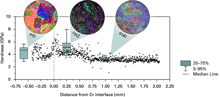
Figure 5. Hardness profile across the laser-clad cross-section from a line scan of 825 indents over 2475 μm. Overlaid box-and-whisker plots correspond to hardness distributions from EBSD-targeted maps at the indicated distances; IPF insets reference local microstructures. Image Credit: Bruker Nano Surfaces and Metrology
PI 89 Auto Enables Efficient Structure-Property Correlation
PI 89 Auto facilitates direct, microstructure-targeted nanoindentation in the SEM through a combination of a patented R/T stage with coordinate-aware software tethered to EBSD/EDS.
The study on laser-clad 410/4140 steel presented here used PI 89 Auto to reveal phase-dependent hardness variations and mechanical gradients across interfaces.
Data collection was performed in a single workday and incorporated three EBSD-targeted XPM maps and one line scan. It took two hours to acquire the XPM grid (dominated by EBSD scan time), and the line scan took ~1.5 hours.
A significant improvement is clear using an automated correlative workflow compared to conventional multi-instrument sequences.
References and Further Reading
- Haake III, J.M. and Zediker, M.S. (2005). Heat treating and cladding operations with high-power diode lasers. SPIE Proceedings, 5706, pp.76–86. DOI: 10.1117/12.601647. https://www.spiedigitallibrary.org/conference-proceedings-of-spie/5706/0000/Heat-treating-and-cladding-operations-with-high-power-diode-lasers/10.1117/12.601647.full.
- Hintsala, E.D., Hangen, U., and Stauffer, D.D. (2018). High-Throughput Nanoindentation for Statistical and Spatial Property Determination. JOM, 70(4), pp.494–503. DOI: 10.1007/s11837-018-2752-0. https://link.springer.com/article/10.1007/s11837-018-2752-0.

This information has been sourced, reviewed, and adapted from materials provided by Bruker Nano Surfaces and Metrology.
For more information on this source, please visit Bruker Nano Surfaces and Metrology.