Hybrid bonding is becoming more critical for advanced semiconductor packaging, thanks to its ability to enable high-density interconnects inside complex 3D assemblies. This approach involves the direct, adhesive-free bonding of two semiconductor surfaces with dielectric and metal regions.
Obtaining a reliable bond requires both surfaces to be pristine. Contributing to this criterion, metrology approaches such as atomic force microscopy (AFM) and atomic force profilometry (AFP) are crucial for characterizing surfaces and optimizing processes.
AFM produces localized, high-resolution surface measurements. Meanwhile, AFP offers complementary large-area topography scans ranging from nanometer-scale characteristics to complete wafer dimensions, including the bevel edge. This article underlines how Bruker’s InSight® 300 AFM and InSight AFP automated solutions deliver multi-scale surface information that informs surface conditioning decisions, improving hybrid bond integrity and device performance.
Hybrid Bonding Overview
The design and manufacturing approach called system technology co-optimization (STCO) is characterized by different chip functions (e.g., memory, I/O, and logic) that are built individually utilizing the most appropriate technologies for each. These parts are fitted together using advanced packaging approaches, including hybrid bonding. Enabling high-density 3D connections among chips, hybrid bonding helps continue performance scaling beyond conventional transistor miniaturization's typical constraints.
Optimal hybrid bonding depends on pristine surface conditions, no matter the approach - wafer-to-wafer, die-to-wafer, or die-to-die. At the local level, crucial metrics include defectivity, surface roughness, and copper contact pad recess depth. All of these need to be tightly monitored. At larger length scales (100 µm and above), surface topography should fall within certain criteria to guarantee appropriate bonding at the wafer interiors and bevel edges alike.
As the most recent generation in a three-decade series of inline AFM and AFP solutions, Bruker’s fully automated InSight 300 and InSight AFP systems stand at the edge of innovations in semiconductor manufacturing by facilitating the precise, scalable characterization of surfaces for next-generation packaging.
Alongside angstrom-level sensitivity and lateral scan sizes that span tens of nanometers to hundreds of millimeters, these platforms aid inline metrology in the complete range of scales needed for hybrid bonding.
Bond Pad Metrology
For proper hybrid bonding, the topmost dielectric surface and the embedded metal bonding pads should accord with stringent topographic criteria. The dielectric should be exceedingly smooth and have a low Rq (root mean square roughness) between 0.1 and 0.2 nm1. It should also have a topographic tolerance considerably more constricted than traditional back-end-of-line (BEOL) dielectric layers.
On the same surface, the metal bonding pads should also be precisely recessed within the dielectric to allow controlled thermal expansion. The usual recess depth for widespread hybrid bond pad sizes sits at a few nanometers (1–5 nm).2,3 These tolerances extend beyond traditional microscopy-based metrology's constraints, making AFM extremely valuable for reaching the high resolution and precision needed for verification processes.
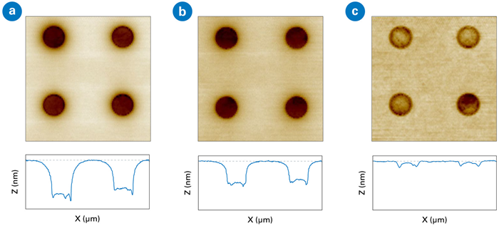
Figure 1. AFM topography scans of four copper pads after three distinct CMP processes, producing different recess depths. The vertical axis is the same for (a-c), visually showing the change in recess depth. Image Credit: Bruker Nano Surfaces and Metrology
High-resolution AFM images in Figure 1 demonstrate four copper contacts that have been scanned following three unique chemical-mechanical planarization (CMP) process skews. These scans show AFM’s sensitivity to multiple important metrics that should be tracked for proper hybrid bonding: dielectric roughness, copper pad roughness, and copper pad recess.
Cross-section profiles in the lower couple of copper pads show high sensitivity to small variations in pad depth for the different CMP processes. Such a level of detail, attained via local AFM scans, produces the metrology information required for developing processes and for tracking excursions in statistical process control (SPC).
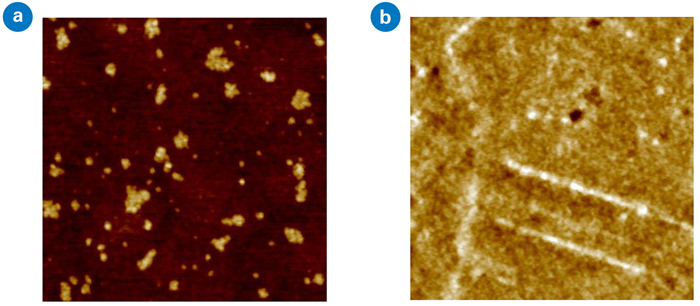
Figure 2. High-resolution AFM scans (1x1 μm) of (a) dielectric and (b) copper pad that show roughness and defects such as small pits and protrusions. Image Credit: Bruker Nano Surfaces and Metrology
Alongside roughness and recess topography, nanoscale defectivity (e.g., pits and protrusions) can greatly affect bond integrity. High-resolution AFM is extremely effective at resolving the pits and protrusions that may constrain yields at the bonding stage. Figure 2a and b display AFM images of dielectric with protrusion growth and copper pad alongside pitting. Distinguishing and reducing these defects is critical, as they can bring voids among the bonding surfaces that reduce device performance or lead to device failure.
Large-Area Scanning
The largest possible field of view for conventional AFMs is around 100 µm2. Such a size is acceptable for localized metrology of dielectrics, Cu pads, and defects discussed above. However, topographical features that span much larger length scales, down to millimeters, have been confirmed by post-bonding approaches, including confocal scanning acoustic microscopy (CSAM), to have a negative effect on wafer-to-wafer bonding. With this in mind, identifying, characterizing, and reducing these topographical excursions in the prebonding step becomes critical.
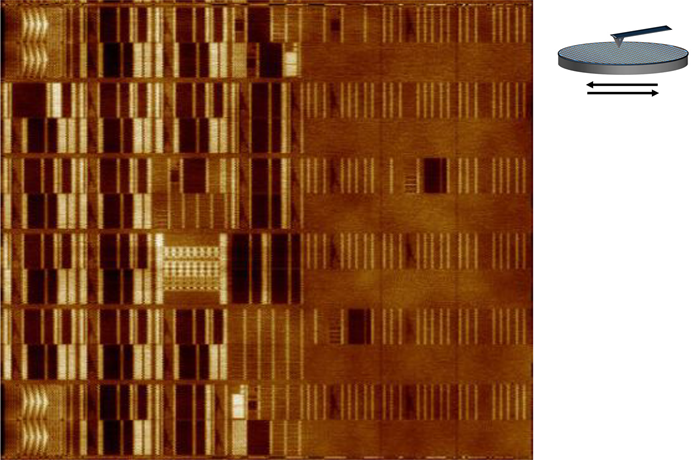
Figure 3. LAS topography image covering 33x26 mm, along with a schematic showing LAS scanning method. Image Credit: Bruker Nano Surfaces and Metrology
Bruker’s Insight AFP system utilizes a proprietary approach called Large-Area Scanning (LAS), which facilitates surface metrology with AFM height sensitivity spanning hundreds of millimeters. In LAS, the wafer sample is raster scanned under the probe. The example 33x26 mm LAS image in Figure 3 demonstrates excessive topography at the multi-millimeter scale.
This is despite the fact that local AFM scans have confirmed dielectric roughness and copper pad recess that accord with the necessary criteria. Further analysis, putting these excessive topography areas into context with circuit design and earlier process stages, also helped the CMP module adjust polishing parameters to minimize topography and ensure proper bonding.
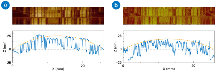
Figure 4. Large-area scans of the same 26x5 mm wafer area (a) before and (b) after topography fabrication mitigation techniques. Image Credit: Bruker Nano Surfaces and Metrology
The LAS capability informs process decisions that minimize large-scale macroscopic topography present above high-metal-density areas, ultimately enhancing wafer bonding and improving yield.
Figure 4a and b demonstrate the same area imaged with the same recipe, scanned prior to and following CMP process improvement. The change generated a significant reduction in long-range topography from 25 nm to 15 nm, as assessed by AFP.
Bevel Edge Metrology
Alongside monitoring local bond pad features and long-range surface topography, assessing the wafer bevel edge is critical for success in wafer-to-wafer hybrid bonding. The top and bottom wafers together need to have properly engineered edge profiles; if the top wafer is not sufficiently trimmed or the bevel topography is insufficiently controlled, upcoming processing stages may not form the structures appropriate for device completion.4
Wafer edge roll-off (ERO) is a central concern at the bevel. ERO is the wafer edge’s precisely engineered curvature. Excursions from the desired, engineered ERO can result in nonuniform bond strength, higher levels of defectivity, and less reliability and yield. AFP is special among ERO monitoring approaches for its better mix of spatial and vertical resolution alongside high-speed profiling. These capabilities facilitate single-nanometer precision (<10 nm) and the high throughput (>45 WPH, 8 sites) that is needed for applications in HVM ERO metrology.
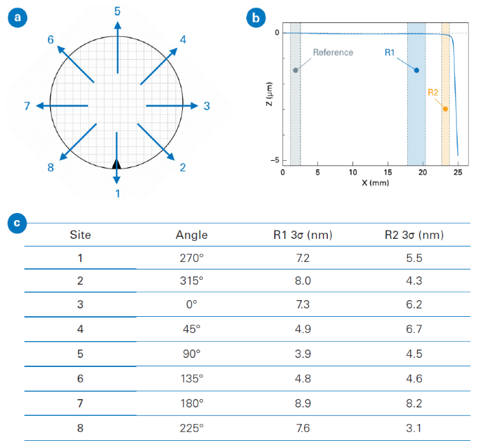
Figure 5. (a) Schematic of ERO measurement sites at 45° angular separation. (b) Bevel-edge analysis comparing Δh between two reference regions, R1 and R2. (c) Exemplary R1 and R2 precision (3σ) for an ERO application. Image Credit: Bruker Nano Surfaces and Metrology
Figure 5a demonstrates a typical ERO measurement of eight sites standing at 45° angular separation. The bevel edge profile length is typically between 10 and 25 mm, assessed at maximum speeds of 25 mm/s. Automated bevel edge characterization analysis, carried out via NanoScope® software, includes Δh calculations between two measurement areas and a reference area. An example analysis alongside results are demonstrated in Figure 5b and c.
The InSight AFP system additionally supports profiling along the full 300 mm wafer diameter, with maximum scan speeds of 25 mm/s, enabling throughput of tens of wafers every hour. Multiple radial profiles can be combined to produce a topographical heat map of a large wafer area.
AFM and AFP Ensure Reliable Hybrid Bonding
Hybrid bonding is fueling high-density 3D integration in sophisticated semiconductor packaging, with success depending on pristine surfaces spanning scales. Bruker’s InSight 300 and InSight AFP systems deliver the multi-scale metrology abilities required to resolve nanoscale defectivity and copper pad recess, characterizing millimeter-scale topography and bevel edge profiles.
By delivering actionable data for developing processes, SPC monitoring, and yield optimization, these tools allow manufacturers to meet the demands of system technology co-optimization and deliver reliable and high-performing device integration.
Acknowledgments
Produced from materials originally authored by Sean Hand, Bruker Senior Staff Applications Scientist and Peter De Wolf, Ph.D., Bruker Sr Director of Technology and Application Development.
References and Further Reading
- Abdilla, J. (2023). Chip to Wafer Hybrid Bonding Development for High Volume Manufacturing. IMAPSource Proceedings, 2023(DPC). https://doi.org/10.4071/001c.90682.
- Ren, H., Yang, Y.-T. and Iyer, S.S. (2022). Recess Effect Study and Process Optimization of Sub-10 μm Pitch Die-to-wafer Hybrid Bonding. 2022 IEEE 72nd Electronic Components and Technology Conference (ECTC), pp.149–156. https://doi.org/10.1109/ectc51906.2022.00034.
- Lu, M.-C. (2024). Hybrid Bonding for Ultra-High-Density Interconnect. Journal of Electronic Packaging, 146(3). https://doi.org/10.1115/1.4064750.
- Kim, Y.-S., Thanh Hai Nguyen and Choa, S. (2022). Enhancement of the Bond Strength and Reduction of Wafer Edge Voids in Hybrid Bonding. Micromachines, (online) 13(4), pp.537–537. https://doi.org/10.3390/mi13040537.

This information has been sourced, reviewed and adapted from materials provided by Bruker Nano Surfaces and Metrology.
For more information on this source, please visit Bruker Nano Surfaces and Metrology.