Sponsored by LuxorReviewed by Ify IsiborJun 24 2026
Nanofibers are fibers with diameters in the nanometer range. They can be produced from various polymers, leading to diverse physical properties and potential applications. Natural polymers include collagen, cellulose, and polysaccharides such as chitosan and alginate, while synthetic polymers include PLA, PCL, PU, PLGA, and PEVA.
The diameter of nanofibers varies based on both the polymer type and the production technique used, with sizes ranging from less than thirty nm to a few hundred nm. Polymer nanofibers are distinctive due to their high surface-area-to-volume ratio, considerable porosity, notable mechanical strength, and flexibility in functionalization when compared to their microfiber equivalents.
Numerous techniques exist for producing nanofibers, including drawing, electrospinning, self-assembly, template synthesis, and thermal-induced phase separation.
Among these, electrospinning is the most widely adopted method, primarily due to its straightforward setup, ability to continuously mass-produce nanofibers from various polymers, and capacity to create ultra-thin fibers with adjustable diameters, compositions, and orientations. This versatility facilitates the customization of fiber shape and arrangement to suit specific application needs.
Nanofibers have a myriad of potential commercial and technological applications. They find use in tissue engineering, drug delivery, cancer detection, lithium batteries, oil-water separation, sportswear textiles, optical sensors, and air filtration
Why is SEM Imaging Used for Nanofiber Study?
SEM imaging of nanofibers serves as an ideal tool for assessing the uniformity and dimensions of nanofibers. Manufacturers of SEM equipment have developed specialized software solutions for fully automated measurement of fiber diameter distributions.
In air filtration applications, nanofibers are leveraged for their antibacterial properties and effectiveness in trapping nanoparticles. SEM imaging (later combined with EDS chemical microanalysis techniques) is used to evaluate filter efficiency and analyze materials captured on the filter.
Most natural and synthetic polymers exhibit good thermal and electrical insulation properties. As a result, when nanofibers or derived products are scanned by an electron beam in a microscope, sample charging can frequently occur.
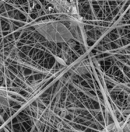
Image Credit: Luxor
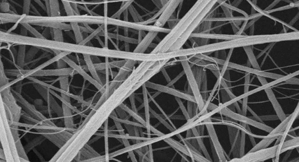
Image Credit: Luxor
Understanding Sample Charging
SEM images are produced by scanning an electron beam over the sample, which effectively adds electrons to the material. Sample charging occurs when there is insufficient electrical conductivity in the samples, preventing electrons from flowing from the sample surface to the sample holder.
This may lead to issues such as drift, blurriness, and low contrast, resulting in distorted images. To avoid sample charging, a very thin layer of a conductive material such as gold, platinum or carbon is applied to the specimen’s surface (a process known as sputter coating or carbon coating), enabling electrons to flow freely and reducing charging effects.
Additional benefits of this sputter coating include enhanced secondary electron emission, reduced beam penetration with improved edge resolution, and better protection for samples sensitive to electron beams.
Luxor metal coaters are engineered to automatically apply a uniform and thin conducting layer onto your SEM samples, safeguarding them from charging effects and improving image quality in electron microscopy.
Image Credit: Luxor
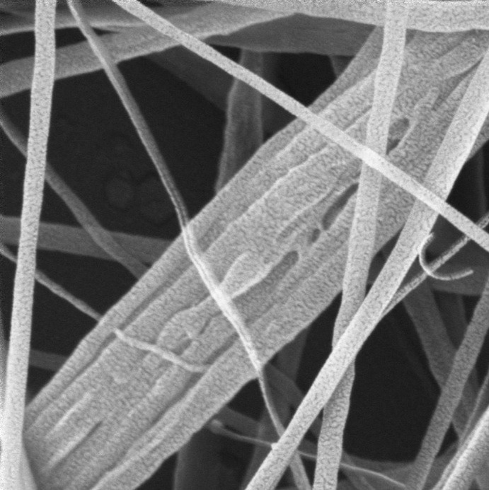
Nanofibers coated 10 nm gold layer - 100.000x magnification. Image Credit: Luxor
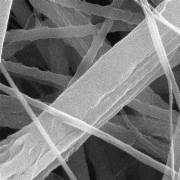
Nanofibers coated 2 nm platinum layer - 100.000x magnification (gold particles in the coating are visible). Image Credit: Luxor
Why Choose LUXOR?
A2 Technology: Precision Coating for High-Resolution Imaging
LUXOR’s A² technology generates a highly stable and precisely controlled plasma, enabling the deposition of thin, uniform coatings. The process starts by evacuating the chamber to create a vacuum, after which a proces gas or air is injected and a high voltage is applied to ionize the gas, initiating the plasma and the coating curent.
To maintain process stability, the coating current is continuously regulated through the controlled high-speed injection of small amounts of process gas into the chamber. This dynamic adjustment ensures that the target current is reached quickly and maintained throughout the coating cycle.
What sets LUXOR metal coaters apart from other commercially available systems is their distinctive approach to process monitoring and control, which provides exceptional precision and reproducibility.
For SEM operators, this translates into acquiring more consistent, uniform metal coatings that significantly improve image quality, enhancing both resolution and contrast.
Moreover, the coating process is fully automated, eliminating manual involvement and ensuring a seamless, hassle-free experience.
Download Luxor's eBook on electron microscopy here
Image Credit: Luxor
Innovative Upside-Down Design for Enhanced Functionality
LUXOR follows a "form follows function" design philosophy, which is reflected in the distinctive architecture of its coaters. Unlike conventional systems, the samples are suspended upside down within the coating chamber, while the target is at the bottom. Although this configuration may initially seem unconventional, it offers several significant practical advantages.
- Safety first: The sputter device has all the high voltage and current lines safely stored within the instrument housing, decreasing the risk of electric shock. This safety function enables the machine to operate with total peace of mind.
- Effortless sample handling: The upside-down design allows for easy access to the lid, which also serves as a loading station for samples. This enables the quick application or removal of samples without the use of special tongs or tweezers. This simplicity not only improves usability but also increases productivity by expediting the process.
- Clean coating process: The clean coating procedure removes loose particles, providing maximum protection for the expensive SEM column. This results in more consistent and reliable outcomes.
- 3D coating: 3D coating improves the coating quality by removing the larger particles towards the pump rather then towards the suspended samples by gravity. LUXOR’s A2 technology eliminates the need for a rotary or planetary table, making it easier to coat three-dimensional, complex and porous samples.
Fully Automated
The coating process is fully automated. Once the samples have been loaded, simply select the appropriate coating thickness and press the Start button. This user-friendly approach significantly reduces the likelihood of human error, and new operators and lab professionals can learn to use the device after only a few minutes of basic instruction.

This information has been sourced, reviewed and adapted from materials provided by Luxor.
For more information on this source, please visit Luxor.