Advanced semiconductor devices depend on intricate 3D architectures made up of diverse material layers, each critical to overall chip performance.
The most popular methods for characterizing these structures are transmission electron microscopy (TEM) and scanning transmission electron microscopy (STEM), which are widely regarded for their excellent spatial resolution.1,2 Furthermore, electron energy loss spectroscopy (EELS) can deliver chemical and bonding data at the nanometer scale by evaluating inelastically scattered electrons.3
To achieve maximum spatial resolution with these methods, samples must be cut into cross-sections thinner than 100 nm. This process is time-consuming and requires costly, specialized equipment, limiting throughput and accessibility.
Even with such extensive sample preparation, EELS is further restricted by the risk of beam damage in organic materials, decreased sensitivity with high-Z elements, and complex data interpretation.3,4
IR PiFM could be an ideal method for characterizing the intricate processes used in the manufacture of sophisticated semiconductor devices. It provides remarkable sensitivity to local chemical bonding information and sub-5 nm spatial resolution in chemical mapping,
To demonstrate this ability, a cross-section (rather than a lamella) was prepared from a power management region of a 3 nm commercially available die/system-on-chip from a consumer wearable device and characterized using IR PiFM.
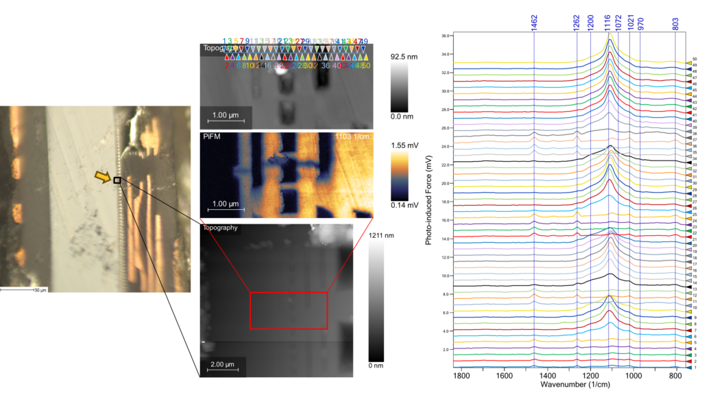
Figure 1. Optical image of the cross-section sample with the region of topography (bottom, 10 mm × 10 mm) indicated by a yellow arrow. A 5 µm × 2 µm region from the center of the lower topography image was analyzed further by acquiring PiF-IR spectra at the locations marked on the upper topography image. The middle image in the column shows the PiFM image acquired at 1103 cm−1, corresponding to the major SiO2 peak, from the same location. Image Credit: Molecular Vista
Figure 1 displays the optical image of the cross-section, AFM topography, and PiFM image, indicating the locations where 50 PiF-IR spectra were collected. These spectra originate from the silicon substrate (spectra 1-5) and span four silicon oxide (spectra 6-10, 14-21, 26-34, and 39-50) and three metallic regions (spectra 11-13, 22-25, and 35-38).
The silicon and metallic regions reveal major siloxane peaks at 803, 1021, 1100, and 1262 cm−1, as well as a C-H bending peak at 1462 cm−1 from a hydrocarbon contaminant. Owing to the greater field enhancement of the tip-enhanced IR light, the peak at 1462 cm−1 is stronger on the metal than on the silicon, making 1462 cm−1 an effective wavenumber for highlighting the metallic region.
From spectrum to spectrum within the oxide regions, the broad silicon oxide peak near 1100 cm−1 shows subtle differences in magnitude, peak position, and shape. These variations likely reflect fluctuations in oxide chemistry at distinct process levels.5 As oxide deposition conditions and available precursors can differ between layers, the local chemistry of silicon oxide can also vary, and PiFM is able to detect those differences.
Figure 2 presents six PiFM images obtained at the same location using different wavenumbers; the top-row images (corresponding to Si–O bonding) appear similar but exhibit minor differences in relative intensity and spatial variations. Again, this likely arises from differences in the growth conditions of the oxide layers.
Inside the red rectangle of the image at 1103 cm−1, three dark regions appear to bridge the metallic layers highlighted in the image at 1460 cm−1.
These regions exhibit higher brightness than the surrounding oxide region yet remain darker than the metallic regions, suggesting the presence of a buried conductive path. This causes the oxide layer above it to be thinner, as evidenced by the reduced signal intensity at the same locations in the oxide-highlighting images.
The images at 970 cm−1 and 1200 cm−1 uncover additional finer features. The image at 970 cm−1 shows a clear, sharp edge around the metallic characteristics, including a roughly 150 nm × 400 nm notch that was significantly less visible in topography. The image at 1200 cm−1 also highlights the suggested conducting material clearly, although the material associated with 1200 cm−1 remains unclear.
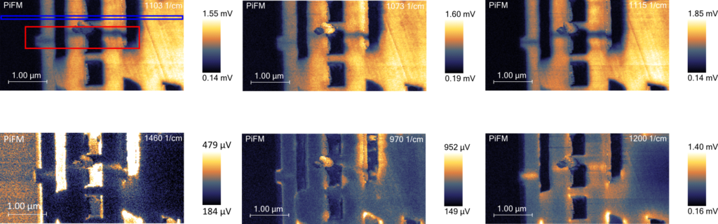
Figure 2. PiFM images at six different wavenumbers from the same location. Image Credit: Molecular Vista
Figure 3 presents the cross-sectional signal-intensity line profiles from the PiFM images in Figure 2. Progressing from the silicon substrate on the left side of the plot toward the subsequent process layers on the right, these profiles corroborate the previous observations and highlight multiple additional features:
- The intensity profiles through each oxide layer show meaningful differences at every measured wavenumber. At 1103 cm−1, the profile is largely symmetrically parabolic, whereas those at 1073 and 1115 cm−1 exhibit opposite, more linear slopes through the layers. These features suggest different processing parameters for oxide deposition.
- The peak at the interface of silicon and the first oxide layer (visible at the 1460 cm−1 profile) suggests the presence of a conducting layer at the interface.
- The profile at 970 cm−1 reveals increased signal near the oxide layer edges, potentially correlating with the precursor chemistry utilized during SiO2 deposition. A peak at 970 cm−1 can be associated with Si–O–C or Si–CH=CH– bonds.
- The line profile at 1200 cm−1 generally aligns with the overall shape of the oxide profiles, indicating that it also shows the oxide. It most resembles the 1073 cm−1 profile, as the slope is positive moving from left to right over the oxide layers.
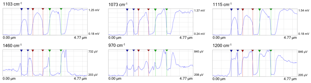
Figure 3. Cross-section signal intensity line profiles of the six images shown in Figure 2, which are all from the region defined by the blue line shown just above the red rectangle in the PiFM image at 1103 cm−1. The top row shows different Si–O bonding configurations, while the bottom row shows the metallic regions and the two wavenumbers highlighting finer features. The first three oxide regions across all images are defined by three pairs of markers (blue, red, and green), which are synchronized across all the line profiles. Image Credit: Molecular Vista
Finally, an investigation into the fine characteristics observed in the images at 970 and 1200 cm−1 was conducted. Figure 4 provides a magnified view of the 800 nm × 800 nm region that contained the observed notch. This view reveals two lobes highlighted at 970 cm−1 alongside the buried conducting material at 1200 cm−1, which connects the conducting interface between the silicon and the first silicon oxide layer to the first metal layer.
While the purpose of the notch remains undetermined, these images illustrate the potential to interrogate the chemical composition of a device through cross-sectioning.
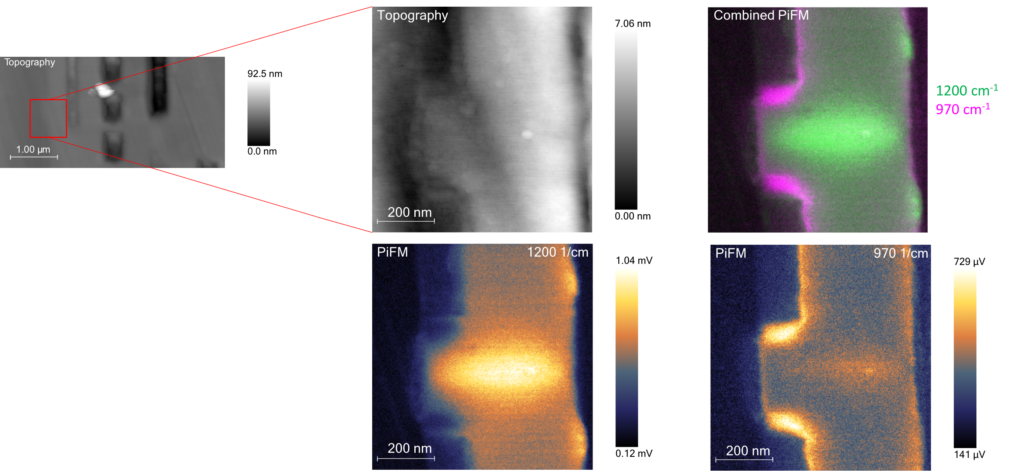
Figure 4. Topography and PiFM images of an 800 nm x 800 nm region containing a “notch” structure into the silicon. Image Credit: Molecular Vista
To conclude, while the proprietary chemistry and processes utilized to create this chip are not accessible, IR PiFM still provides substantial insight into this device. These findings demonstrate that PiFM can differentiate among various oxide forms, locate and identify both particulate and widespread contaminants, and occasionally detect buried features, all while maintaining a significantly high spatial resolution.
References & Further Reading
- NIST. (2023). Advanced Analytical Electron Tomography for Materials Development and Failure Analysis in Semiconductor Devices | NIST. (online) Available at: https://www.nist.gov/programs-projects/advanced-analytical-electron-tomography-materials-development-and-failure-analysis.
- de la Mata, M. and Molina, S.I. (2022). STEM Tools for Semiconductor Characterization: Beyond High-Resolution Imaging. Nanomaterials, 12(3), p.337. DOI: 10.3390/nano12030337. https://www.mdpi.com/2079-4991/12/3/337?utm_source=researchgate.net&utm_medium=article.
- Heller, N.J., Washington, A.J. and Cushing, S.K. (2025). Electron Energy Loss Spectroscopy. ACS In Focus. DOI: 10.1021/acsinfocus.7e9010. https://pubs.acs.org/doi/book/10.1021/acsinfocus.7e9010.
- Egerton, R. (2006). Limitations of Electron Energy-Loss Spectroscopy. Microscopy and Microanalysis, 12(S02), pp.102–103. DOI: 10.1017/s1431927606061885. https://academic.oup.com/mam/article-abstract/12/S02/102/6915156?redirectedFrom=fulltext.
- Chemistry LibreTexts. (2020). 7.11: Oxidation of Silicon. (online) Available at: https://chem.libretexts.org/Bookshelves/Inorganic_Chemistry/Chemistry_of_the_Main_Group_Elements_(Barron)/07%3A_Group_14/7.11%3A_Oxidation_of_Silicon.

This information has been sourced, reviewed, and adapted from materials provided by Molecular Vista.
For more information on this source, please visit Molecular Vista.