Advanced packaging is a relatively new innovation in semiconductor fabrication, in which multiple devices (or dies) are bonded together before being encapsulated.
It has become essential in enabling shorter signal paths, higher interconnection density, and sustaining performance scaling, which together can increase processing speed.1,2
During the production process, one of the most important steps is wafer binding. In this process, single- or multi-layer thin-film via wafers (MTVs) with copper through-silicon vias (TSVs) are temporarily attached to carrier wafers. Corresponding Cu-TSVs are aligned and brought into contact to bind the wafers together, chemically bonding them at the nanoscale. The carrier wafers are then debonded, the bound wafers are cleaned, and the process repeats (Figure 1).
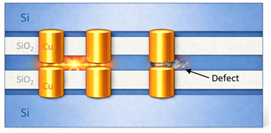
Figure 1. Example diagram illustrating how defects can affect the manufacturing process. Two silicon wafers with embedded Cu-TSVs surrounded by a SiO2 dielectric are being joined through direct Cu-Cu binding. Two Cu-TSVs properly bind (left and middle), but one Cu-TSV does not due to an intervening defect (right). Image Credit: Molecular Vista
Though substantial improvements have been seen in chip performance from advanced packaging systems, the manufacturing process is incredibly intricate and extremely sensitive to surface conditions. Each wafer surface must be exceptionally clean, especially during the binding step, for TSV-to-TSV binding to successfully and reliably occur. The cleaning steps must effectively remove all faults.
Whether introduced during handling or because of cleaning steps being bypassed, even a minute number of residual defects can significantly reduce chip performance further downstream. It is crucial that defects are easily detectable and identifiable during the manufacturing process so that corrective actions can quickly eliminate them. Accordingly, pushing the limits of the optical resolutions of inspection tools is seen as the key to driving further innovation in the semiconductor industry.3
Where PiFM Steps In: A Case Study
Molecular Vista was approached recently by a group that wanted to evaluate their adhesive cleaning process following a carrier wafer debonding step.
After analyzing the topography image centered on a Cu-TSV, they observed two sets of small, spherical features: one faint set had diameters of ~20 nm, and one more prominent set with ~50 nm-sized diameters. However, the two sets’ identities would have remained unclear if only topography was used for analysis, and initially, the team could not assertively classify either of the sets as defects.
Following PiFM analysis, however, the Molecular Vista team was able to prove that the cleaning process had failed. On the cleaned wafer, the ~20 nm-sized group was identified as adhesive residue, and the particles in the ~50 nm-sized group were seen to be aggregations of copper (I) oxide, as a result of the sample’s exposure to air. In addition, the team clearly observed that the adhesive residue was uniformly spread on both the Cu-TSV and the dielectric surface. These conclusions were drawn following imaging that was taken at the different wavenumbers present in the spectra (Figure 2).
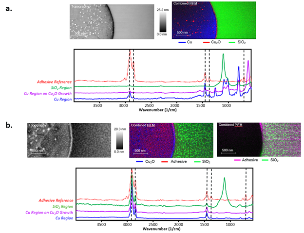
Figure 2. Topography and combined PiFM images of a Cu-TSV cross section for a) the unexposed wafer and b) the exposed and cleaned wafer, as well as PiF-IR spectra acquired along a path from the TSV into the dielectric. Image Credit: Molecular Vista
In this study, the team presents PiFM as a new analytical technique with great promise for detecting defects in semiconductor manufacturing settings, particularly in advanced packaging, within which defect review is especially challenging and important. PiFM can help to distinguish true contaminants from benign morphological features by providing chemical information at the nanoscale to supplement topographical data, supporting fast process optimization.
References
- LaPedus, M. (2021). Advanced Packaging’s Next Wave. (online) Semiconductor Engineering. Available at: https://semiengineering.com/advanced-packagings-next-wave/.
- Moyer, B. (2025). Advanced Packaging Fundamentals for Semiconductor Engineers. (online) Semiconductor Engineering. Available at: https://semiengineering.com/ebook-advanced-packaging-fundamentals-for-semiconductor-engineers-2025/.
- Haley, G. (2025). How Advanced Packaging Is Reshaping Inspection. (online) Semiconductor Engineering. Available at: https://semiengineering.com/how-advanced-packaging-is-reshaping-inspection/.
Acknowledgments
Produced using materials originally authored by Christine Albrecht, Padraic O’Reilly, Yun Jing, and Sung Park from Molecular Vista.

This information has been sourced, reviewed, and adapted from materials provided by Molecular Vista.
For more information on this source, please visit Molecular Vista.