Review PiFM (photo-induced force microscopy) on the Vista 300 complements the existing Review SEM (scanning electron microscopy) analysis employed in automated defect review (ADR) by pairing non-destructive measurement with sub-5 nm resolution spectro-chemical and morphological imaging, enabling automated nano-defect review (ANDR).
Owing to progress in semiconductor device architectures, defects as small as 10 nm are now classified as killer defects. Moreover, non-metallic defects increasingly drive yield loss and remain chemically indistinguishable by Review SEM/EDX, the present ADR workhorse.
Review SEM/EDX fails to reliably detect sub-10 nm defects, even when metallic, because low-energy X-ray peaks overlap for numerous metals in semiconductor processes. This article examines how Review PiFM on the Vista 300 addresses Review SEM limitations and integrates into the ADR workflow for defects below 10 nm.
How PiFM Complements Review SEM
PiFM enhances current ADR instrumentation by delivering non-destructive measurement and chemical identification for defects that are either too small (sub-10 nm) or organic.
Review SEM/EDX is often applied in wafer defect review; however, electron-beam bombardment from SEM/EDX damages sub-20 nm and organic defects. Figure 1 illustrates two destruction modes observed with PiFM on wafer defects following SEM/EDX analysis.
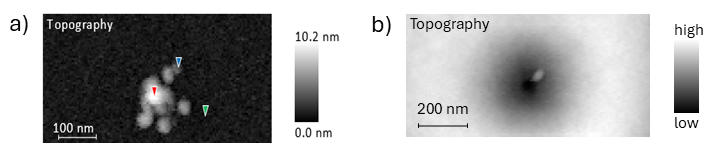
Figure 1. PiFM topography images show damage from e-beam analysis on wafer defects. a) Defect fragmentation due to e-beam analysis. b) Complete obliteration of a defect due to e-beam analysis. Image Credit: Molecular Vista
Destructive measurement prevents re-examination of defects with alternative techniques and limits the operator’s ability to gather complete data. PiFM merges non-contact atomic force microscopy (AFM) with infrared (IR) spectroscopy. By functioning in non-contact mode, Molecular Vista instruments keep the AFM probe within the attractive region of the van der Waals potential between probe and sample surface, guaranteeing that tip and surface stay undamaged and uncontaminated. Non-contact operation affords the operator the chance to revisit defects of interest (DOI).
For defects under 20 nm, electron beam energies below 3 keV are required to shrink the interaction volume in EDX measurements. At such energies, however, the principal peaks that distinguish X-ray families are unresolved, yielding only a single dominant peak.
Figure 2 directly demonstrates this failure mode: characteristic peaks of Si (silicon), W (tungsten), Rb (rubidium), and other present elements lie sufficiently close in energy to coalesce into one unresolved feature, preventing confident assignment of any single element.
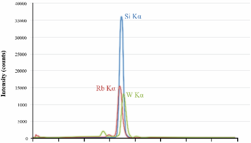
Figure 2. Overlapping EDX x-ray peaks of Si, W, Rb, and other metals. Image Credit: Molecular Vista
As defects diminish to the sub-20 nm scale, EDX-based composition becomes indeterminate. Lastly, for organic defects, elemental composition alone cannot identify compounds, even if the defect survives electron-beam interrogation.
PiF-IR spectroscopy circumvents the EDX constraints outlined above. Since photo-induced force detection is a near-field phenomenon confined to the tip–sample junction, the sampled volume is defined by the tip apex rather than by electron-beam penetration. Therefore, the acquired spectrum represents only the particle, not adjacent material.
Furthermore, PiF-IR probes vibrational absorption rather than electronic transitions, permitting molecular species identification. Figure 3 presents the PiF-IR spectrum obtained with a Vista series instrument on a 15 nm particle atop the underlying quartz substrate.
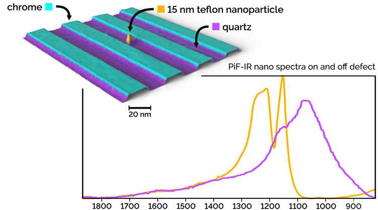
Figure 3. An artistic rendering of an actual PiFM chemical map shows a 15 nm Teflon particle at the center of the line-space pattern. Spectra on and off the defect clearly identify the particle as Teflon and distinguish it from the quartz line. Image Credit: Molecular Vista
Where EDX would yield an ambiguous, blended signal, PiFM delivers an unambiguous molecular ID, in this instance, a Teflon particle. PiFM unites three ANDR capabilities unattainable by SEM/EDX: non-destructive measurement, molecular identification, and high spatial resolution with height data.
The ANDR Workflow with PiFM
PiFM on the Vista 300 integrates into standard fab inspection workflows by ingesting defect coordinate maps (e.g., KLARF) directly from inline inspection tools, auto-deskewing to wafer fiducials (typically a few larger defects), and visiting each defect of interest (DOI) sequentially to collect topography and PiF-IR spectra.
Figure 4 shows a workflow diagram for Review PiFM. Typical throughput on the Vista 300 is roughly two minutes per defect, contingent on coordinate accuracy from the inspection tool, allowing chemical-ID surveys of about 30 defects per hour.
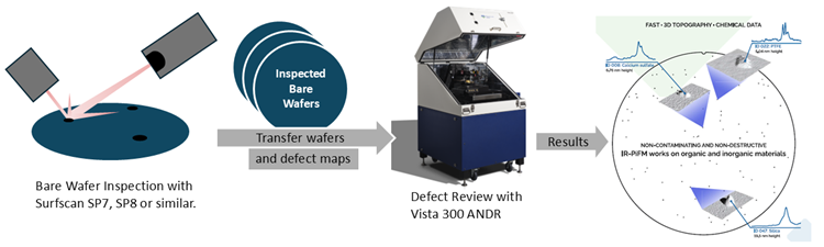
Figure 4. Typical ANDR workflow with Review PiFM. Wafers with small or organic defects are routed to the Vista. Image Credit: Molecular Vista
Owing to its modest throughput, PiFM is not intended as a full replacement for SEM/EDX but functions alongside those systems. Present SEM/EDX tools achieve an order-of-magnitude higher throughput than Vista 300 ANDR.
Consequently, when numerous larger inorganic/metallic defects require binning by shape and elemental content, SEM/EDX remains the workhorse. Nevertheless, defects that SEM/EDX cannot classify effectively should be directed to the Vista 300 ANDR for PiFM analysis.
This strategy lessens the need for time-intensive, destructive follow-up using ToF-SIMS or TEM/EELS.
PiFM Distinguishes Identical Particle Defects
Similar to SEM, PiFM topography images can detect surface particles with excellent lateral resolution. Morphology alone, however, is insufficient to ascertain a particle’s composition and thus the root cause of defectivity.
Determining the origin of a defect class requires knowledge of the defect’s chemical composition. Figure 5 shows an example from a study performed with CT Associates: two particles of identical size and shape appear on the substrate. Without chemical analysis, one might incorrectly conclude these particles share a common source.
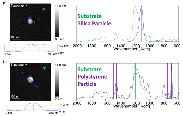
Figure 5. Two apparently identically sized and shaped particle defects on a bare wafer. PiF-IR spectra identify the defect in (a) as a silica particle and the defect in (b) as a polystyrene particle. Image Credit: Molecular Vista
PiF-IR spectra acquired on the particles rapidly identify them as silica and polystyrene, clearly indicating distinct origins. Here, Review PiFM analysis provides information that Review SEM cannot: differentiation between identically shaped particles, which accelerates progression to the next root cause analysis step.
PiFM can also detect particles smaller than 10 nm. In Figure 6, PiFM analysis clearly reveals a 5 nm particle on the silicon substrate. Particle size and height are derived from PiFM topography images, while chemical composition is established by collecting PiF-IR spectra and comparing them to reference FTIR spectra of bulk material.
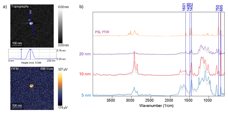
Figure 6. a) AFM topography, horizontal line trace displaying the shape and height, and PiFM chemical map of a 5 nm defect on a silicon wafer. b) FTIR reference spectrum (4) of PSL displayed with PiF-IR spectra from similar composition defects on the same wafer ranging in size from 5–20 nm. By comparison to the reference spectra, these particles are identified as PSL. Image Credit: Molecular Vista
In this case, the 5 nm particle is identified as PSL, providing another demonstration of PiFM’s utility in defect review. Even particles far below EDX’s spatial resolution can be identified with PiFM.
Summary of the Capabilities of Review PiFM
Review PiFM expands automated defect review to sub-10 nm and organic defect types critical for shrinking device structures and unaddressable by Review SEM/EDX. By combining non-contact AFM topography with IR spectroscopy, the Vista 300 reports height, shape, and molecular identity of defects below 5 nm without causing damage.
The examples above illustrate capabilities beyond SEM/EDX: unambiguous identification of a 15 nm Teflon particle, discrimination between identically shaped silica and polystyrene particles, and chemical identification of a 5 nm PSL particle.
Because SEM/EDX retains an order-of-magnitude throughput advantage, the two techniques are optimally deployed in tandem, with defects unclassifiable by SEM/EDX routed to the Vista 300 for PiFM analysis.
When employed in this way, ANDR with Review PiFM shortens the path from defect detection to root cause and reduces dependence on speculative, destructive follow-up methods.
References and Further Reading
- CT Associates, Inc. (n.d.) CT Associates, Inc. Available at: https://www.ctassociatesinc.com/
- Nowak, D., et al. (2016) Nanoscale chemical imaging by photoinduced force microscopy, Science Advances, 2(3), p. e1501571. DOI: 10.1126/sciadv.1501571. https://www.science.org/doi/10.1126/sciadv.1501571
- Molecular Vista (2026) Root cause analysis for semiconductor wafer contamination: identifying sub-20 nm organic and inorganic defects with PiFM. Available at: https://molecularvista.com/applications/root-cause-analysis-for-semiconductor-wafer-contamination-identifying-sub-20-nm-organic-and-inorganic-defects-with-pifm/
- Wiley Science Solutions. KnowItAll IR Spectral Database Collection. Available at: https://sciencesolutions.wiley.com/solutions/mark/knowitall/

This information has been sourced, reviewed, and adapted from materials provided by Molecular Vista.
For more information on this source, please visit Molecular Vista.