Semiconductor devices are becoming smaller, faster, and more complex, placing greater demands on the tools used to manufacture, inspect, and characterize them. From high-resolution patterning to advanced defect detection, the industry is continually developing new methods to maintain performance, reliability, and production efficiency.
This Semiconductor Analysis & Manufacturing Industry Focus eBook features insights into the fabrication techniques, analytical methods, and emerging materials helping shape the next generation of semiconductor research and manufacturing.
Download the eBook
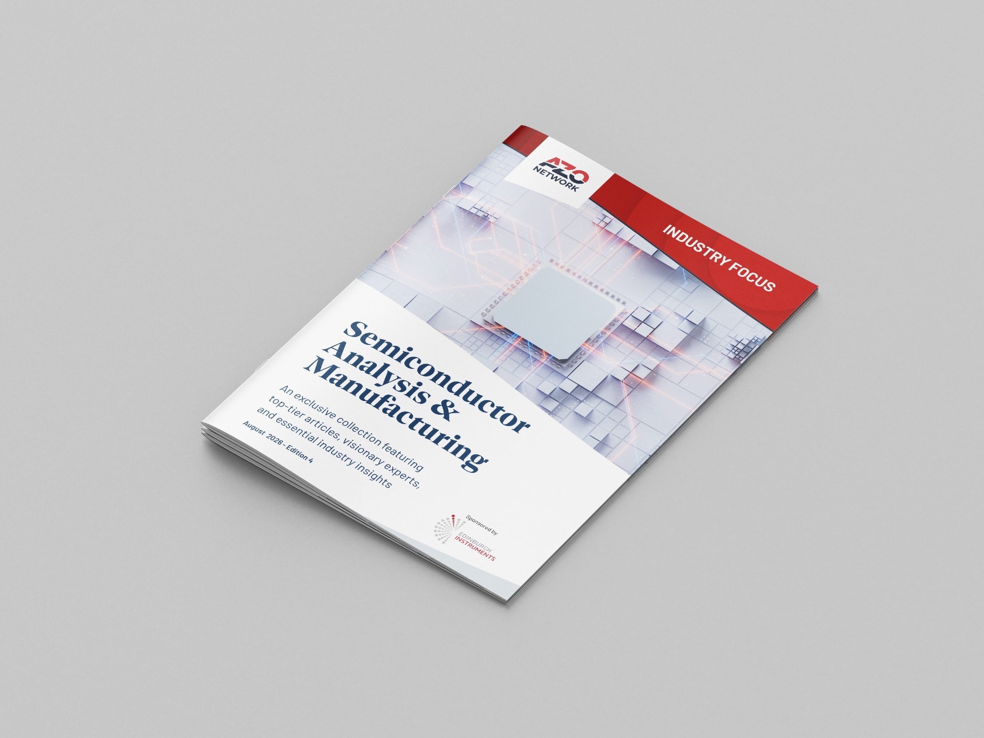
Here’s a quick look at what’s inside:
- How nanoimprint lithography enables high-resolution, scalable semiconductor patterning
- New printing methods for creating denser nanowire arrays in flexible electronics
- The use of Raman and photoluminescence techniques to characterize semiconductor materials
- Advanced optical and electron-beam approaches for wafer inspection and defect detection
- How multimodal analysis can provide deeper insight into two-dimensional semiconductors
Download the eBook
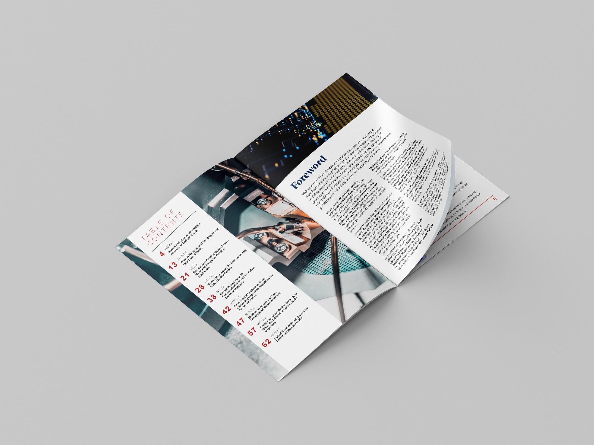
The eBook also explores the growing importance of materials characterization. Complementary optical techniques can reveal valuable information about gallium nitride, while precise atomic processes are opening new possibilities for tuning two-dimensional semiconductor alloys for future quantum technologies.
These articles provide a general overview of tools, materials, and manufacturing approaches driving progress across semiconductor research, development, and high-volume production. Whether you work in fabrication, inspection, materials analysis, or quality control, this eBook provides timely insights into the technologies supporting continued semiconductor innovation.

This information has been sourced, reviewed, and adapted from materials provided by Edinburgh Instruments.
For more information on this source, please visit Edinburgh Instruments.