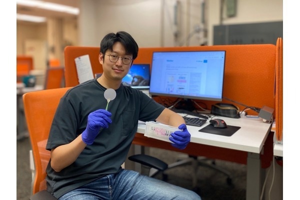
Researchers at the University of Pennsylvania School of Engineering and Applied Science have grown a high-performing 2D semiconductor to a full-size, industrial-scale wafer. In addition, the semiconductor material, indium selenide (InSe), can be deposited at temperatures low enough to integrate with a silicon chip. (Pictured above: Seunguk Song). Image Credit: University of Pennsylvania
For these demands to be fulfilled, the industry should look beyond silicon to produce devices suitable for the increasing scope of computing.
Although it is unlikely that the technology sector will completely replace the current dominant materials anytime soon or in the near future, there will be a need for innovative improvements in chip materials and designs. These enhancements are necessary to meet the evolving demands of computing technology.
One of the major defects of silicon is that it cannot be made so thin since its material properties are restricted to three dimensions. For this cause, two-dimensional semiconductors—so thin as to have nearly no height—have turned out to be an object of interest to engineers, researchers, and microelectronics manufacturers.
Thinner chip components would offer huge control and accuracy over the flow of electricity in a device while reducing the amount of energy needed to power it. Also, a 2D semiconductor would add up to keeping the surface area of a chip to a minimum, lying in a thin film atop an assisting silicon device.
However, until now, measures taken to create such a material have not been successful.
Some 2D semiconductors have shown good individual performance but needed extremely high temperatures for deposition, which could damage the underlying silicon chip. Others could be deposited at temperatures compatible with silicon, but their electronic properties, such as energy efficiency, speed, and precision, were subpar. Some met the temperature and performance criteria but could not achieve the necessary level of purity at industry-standard sizes.
Now, scientists at the University of Pennsylvania School of Engineering and Applied Science have grown a high-performing 2D semiconductor to a full-size, industrial-scale wafer. Besides, the indium selenide (InSe), a semiconductor material, could be deposited at temperatures low enough to combine with a silicon chip.
Deep Jariwala, Associate Professor and Peter and Susanne Armstrong Distinguished Scholar in the Department of Electrical and Systems Engineering (ESE), and Seunguk Song, Postdoctoral Fellow in ESE, headed the study, reported recently in Matter.
Semiconductor manufacturing is an industrial-scale manufacturing process. You aren’t going to have a viable material unless you can produce it on industrial-scale wafers. The more chips you can make in a batch, the lower the price. But the material must also be pure to ensure performance. This is why silicon is so prevalent — you can make it in large quantities without sacrificing purity.
Deep Jariwala, Associate Professor and Peter and Susanne Armstrong Distinguished Scholar, Department of Electrical and Systems Engineering, School of Engineering and Applied Science, University of Pennsylvania
InSe has for a long time shown promise as a 2D material for robust computing chips since it carries electrical charge exceedingly well.
However, producing large films of InSe has proven difficult since the chemistry of selenium and indium tends to integrate in a few various molecular proportions, taking on chemical structures with altering ratios of every element and hence compromising its purity.
The success of the research group depended on Song’s application of a growth method that overcame the whims of InSe’s atomic structure.
For the purposes of an advanced computing technology, the chemical structure of 2D InSe needs to be exactly 50:50 between the two elements. The resulting material needs a uniform chemical structure over a large area to work.
Seunguk Song, Postdoctoral Fellow, Electrical and Systems Engineering, School of Engineering and Applied Science, University of Pennsylvania
The research group achieved this innovative purity utilizing a growth method known as “vertical metal-organic chemical vapor deposition” (MOCVD). Earlier studies have attempted to simultaneously introduce selenium and indium in equal quantities.
But Song illustrated that this technique was the source of unwanted chemical structures in the material, thereby generating molecules with altering ratios of every element. In opposition, MOCVD functions by transmitting the indium in a constant stream while introducing the selenium in pulses.
By pulsing, you give the indium and selenium time to combine. In the moments between pulses, you deprive the environment of selenium, which prevents the ratio from getting too high. The benefit of the pulse is the pause. That’s how we get a uniform 50:50 ratio across our entire full-size wafer.
Seunguk Song, Postdoctoral Fellow, Electrical and Systems Engineering, School of Engineering and Applied Science, University of Pennsylvania
Apart from ensuring the chemical purity of the material, the research team was also able to manage and align the orientation of crystals within it. This additional control and alignment significantly improved the quality of their semiconductor by creating a flawless environment for the movement of electrons.
“The two most important material qualities in a semiconductor are chemical purity and crystalline order. The most important industrial quality is scalability. This material checks every box,” states Jariwala.
Journal Reference
Song, S., et al. (2023). Wafer-scale growth of two-dimensional, phase-pure InSe. Matter. doi.org/10.1016/j.matt.2023.07.012.