Bruker today announced the launch of two groundbreaking detectors at Microscopy & Microanalysis (M&M) 2026: the eWARP™ TKD, a next-generation Transmission Kikuchi Diffraction (TKD) detector for nanoscale crystallographic characterization, and the XFlash® FlatQUAD™ 2L, the latest evolution of Bruker’s annular EDS detector, enabling simultaneous Energy Dispersive X-ray Spectroscopy (EDS) and Back-Scattered Electron (BSE) detection. These innovations redefine the possibilities of Scanning Electron Microscope (SEM)-based characterization by compounding breakthrough speed, sensitivity, spatial resolution, and multimodal analytical capabilities.
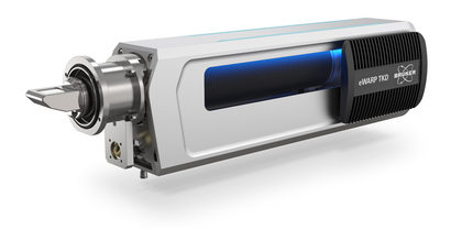 New eWARP TKD detector for unmatched throughput, resolution and quality in nanomaterials characterization. Image Credit: Bruker Nano GmbH – Electron Microscope Analyzers
Building on Bruker’s unique eWARP technology, the eWARP TKD brings the advantages of Direct Electron Detection (DED) with Wide ARea Pixelated (WARP) sensors to TKD in SEMs. The detector combines a new 162 × 162 pixel sensor with a large 26 × 26 mm2 active area and acquisition speeds up to 5,700 frames per second for unprecedented productivity and data quality. Exceptional sensitivity and ultrafast readout enable the acquisition of diffraction data up to an order of magnitude faster than with conventional TKD. Combined with a state-of-the-art field-emission SEM, eWARP TKD delivers sub-2 nm spatial resolution, enabling researchers to characterize semiconductor structures, thin films, 2D materials, energy materials, and nanostructured alloys acquired over larger areas than before. Bruker’s patented on-chip binning allows integrated Dark-Field- and Bright-Field-like imaging at unmatched speed, providing complementary microstructural information and real-time observation of material changes during in-situ experiments.
The new XFlash® FlatQUAD™ 2L enables industry-leading EDS efficiency with simultaneous BSE imaging. Utilizing Bruker’s unique annular four-segment Silicon Drift Detector (SDD) between SEM pole piece and sample, the XFlash® FlatQUAD 2L enables direct correlation of elemental composition and contrast. Acquiring EDS and BSE simultaneously accelerates characterization workflows, reduces electron dose on sensitive samples, and obtains perfectly co-registered multimodal datasets. The combination is particularly valuable for heterogeneous and multiphase materials, semiconductor devices, battery electrodes, nanoparticles, biological specimens, and FIB lamellae, where rapid identification of elemental distributions, interfaces, contamination, coatings, defects, and degradation mechanisms is critical.
“The eWARP TKD represents a major leap forward in quantitative nanoscale characterization in SEMs,” said Daniel Goran, Senior Product Manager EBSD at Bruker. “By combining DED with our industry-leading on-axis TKD approach, the eWARP TKD allows researchers to characterize nanostructured materials faster, over larger areas, and with greater confidence than ever before.”
“The XFlash® FlatQUAD 2L changes the acquisition of analytical data in SEMs,” added Andi Kaeppel, Senior Product Manager EDS/SEM at Bruker. “The ability to collect perfectly correlated EDS and BSE information gives a more complete understanding of complex materials, while simplifying and accelerating their workflows.”
These innovations reinforce Bruker’s position at the forefront of SEM detector development, delivering the technologies researchers need to better understand increasingly complex materials and devices.