Deep Level Transient Spectroscopy (DLTS) is considered to be a great tool for characterizing electrically active majority carrier traps in semiconductors [1]. The fundamental principle of DLTS comprises of measuring the capacitance of an ideal junction such as a reverse-biased Schottky diode, while filling biasing voltage pulses are applied.
The majority carriers are swept by the voltage pulses into the volume of the junction, which is originally depleted of mobile charge carriers because of reverse biasing. Here, it could be possible to capture them by electrically active defects. After restoring the initial reverse biasing, the majority carriers that are trapped are progressively released from the electrically active defects, causing a gradual change in capacitance. Measuring this capacitance transient provides a fingerprint of the defects involved in the emitting process.
The amplitude of the transient is associated with the concentration of the defects, while the time constant is linked to their energy level of the defect and capture cross section. A number of numerical procedures are available for extracting these defect properties from the measured capacitance transient. This article presents two basically different procedures: conventional-DLTS (from now on DLTS) and Laplace-DLTS (L-DLTS). In the case of DLTS, the attained signal is multiplied by a weighting function and the output integrated over time, thus resulting in a maximum when the transient time constant corresponds with a known preset value, the so called “rate window”.
In the case of L-DLTS, the Laplace reverse transform of the measured transient is numerically calculated in order to extract the spectral density and also to distinguish individual contributions within the acquired data. This article describes an MFIA-based setup used to carry out the L-DLTS and DLTS measurements, and compares its performance with a commercially available DLTS/L-DLTS system based on the Boonton 7200 [2]. The results show that the MFIA-based setup executes at least on par with the Boonton-based setup. Finally, this article summarizes a few major differences between DLTS and L-DLTS, and establishes that L-DLTS can be considered as a refinement to DLTS.
Setup and Sample
A description of the setup used to carry out the DLTS and L-DLTS characterization is provided in Figure 1. The capacitance was measured in a 4-terminal configuration using the MFIA in the 3 V and 1 mA voltage and current range, respectively. An internal DC offset, Vdc, of -2.8 V was added to the 30 mVrms test signal, Vtest, to reverse bias the Schottky diode. The negative biasing DC voltage, Vdc, was superimposed with 100 ms pulses of 2.8 V (Vp) provided by a pulse generator (Agilent 33220A) and then fed into Aux Input 1 of the MFIA. Additionally, the sync signal output of the pulse generator was coupled to the MFIA back panel Trigger Input 1 in order to synchronize pulse generation with transient acquisition. The MFIA was controlled and data was attained, using LabView.
The sample comprises of a Pd-ZnO Schottky diode realized on a hydrothermally grown ZnO wafer (n-type) [3]. It was installed in a liquid nitrogen cryostat attached to a Lakeshore 332 temperature controller. A compensation step was carried out before acquiring the transients due to significant spurious impedance of the custom fixture and wiring. It is also worth mentioning that, no 180° phase shifted signal was added in order to compensate the constant capacitance component of the Pd-ZnO Schottky diode. This is in contrast to the method reported in the earlier blogpost describing DLTS measurements [1].
In this article, the total sample capacitance was measured during the DLTS/LDLTS characterization while using the MFIA without any voltage-overflow conditions taking place even when the filling pulse was present (this condition has been found to be vital for optimal performance).
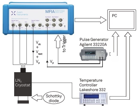
Figure 1. Schematic view of the MFIA-Based DLTS set-up.
DLTS with the MFIA
MFIA vs Boonton 7200
An in depth study was carried out in order to compare the measurements performed with the MFIA-based setup described in Figure 1 and a commercially available DLTS setup based on a Boonton 7200 capacitance meter [2]. Transients attained with these two setups, under equal quiescent conditions (Vdc= -2.8 V, Vp = 2.8 V for 100 ms) and capacitance signal sampling rate (13 kHz) are shown in Figure 2 (a) and (b). Figure 2 displays extremely good correspondence between the two setups for the acquired capacitance, including a similar signal-to-noise ratio (SNR).
Overflow condition does not occur when the pulse is applied while using the MFIA, so the capacitance is also accurately measured during the pulsing release, as shown in Figure 2 (a) and (b). On the contrary, for the measurements executed with the Boonton 7200, a recovery time of ~0.2 ms is observed as a consequence of the overloading during the pulsing time.
Having established the MFIA-based setup performs well compared with the Boonton-based one, a more in depth analysis was carried out using the MFIA-based setup. If only one kind of trap with concentration (Nt) is present in the Schottky diode depletion region, the time, t, and temperature, T, dependence of the capacitance transients, ΔC(T, t), is equal to [4]
 |
(1) |
where C0, Nd and en(T) are the quiescent capacitance of the Schottky diode, donor concentration and the emission rate, respectively, while F is a correcting factor (~1 in ordinary measurements conditions), that considers the actual portion of depletion region investigated during the measurements [4, 5, 6].
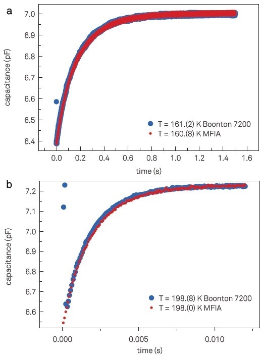
Figure 2. Capacitance transients acquired at 1 MHz, sampling rate 13 kHz, and temperature ~161 K (a) and ~198 K (b) using the MFIA (red dots) and Boonton 7200 in the 2 pF range (blue dots). Data points related to the recovery time from overloading are present on the Boonton 7200 measurements, but the MFIA is not affected.
DLTS vs L-DLTS
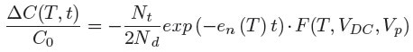
In DLTS, capacitance transients are acquired while the temperature is ramped up or down. The DLTS spectra as a function of temperature, S(T), is acquired by filtering the transient capacitance, averaged in a temperature interval around T, with a weighting function, W(t) i.e. by carrying out the following integral:
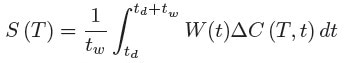 |
(2) |
where td and tw are the delay time (introduced to eradicate the impedance meter overloading) and the time length of the time window, respectively. A maximum in S(T) is obtained when en(T) matches the filter window corresponding to the W(t) chosen. Additionally, from the DLTS spectra peak height 2ΔC/ C0 can be extracted by inverting Equation 2. This quantity is almost equal to the ratio of defect to main donor concentration as can be deduced by looking at Equation 1.
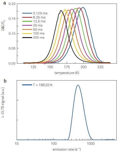
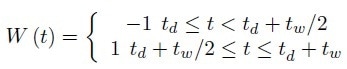
Figure 3. DLTS (a) and L-DLTS (b) spectra acquired with Vdc = -2.8 V, Vp = 2.8 V for 100 ms and capacitance measured at 1 MHz with a sampling rate of 13 kHz. In (a) curves correspond to the different time window lengths, tw, used for W(t) to analyze transients (td = 4 x 10⁻⁴ s in all the measurements). A maximum can be observed occurring, for example, at 198 K for a window length of 3.125 ms. In (b) an L-DLTS spectrum obtained by performing a Laplace numerical inversion of an averaged capacitance transient acquired at T~198K.
The DLTS spectra and an example of such analysis displayed in Figure 3 (a) were obtained by using the following weighting function:
 |
(3) |
Such a function is considered to have the characteristic that the maximum will occur when en(T) ~ (tw/2)-1. It is also important to point out that filtering with this weighting function is principally the difference between the transient averaged over the first and the second half of the time window length. Thus, this approach has the benefit of majorly reducing the noise contribution and increasing sensitivity. As an example, the longest time window acquisition shown in Figure 3(a) comprises of 2500 points. As a consequence of this integration, the SNR is increased by a factor √2500/2 ~ 30 when performing the integrals over the time interval tw/2. This implies a factor ~20 higher SNR in the resulting DLTS spectrum.
By applying the weighting function from Equation 3 to the measured transients, a maximum at 198 K was observed for a window length of 3.125 ms as displayed in Figure 3 (a). This peak specifies the presence of defects. Another approach to analyze the acquired transients is provided by L-DLTS.
For a given transient, the emission rate spectral distribution is obtained by numerically solving the integral:
 |
(4) |
i.e. computing the reverse Laplace transform. This deals with discretization of the integral equation and the solution of the system of equations so obtained. It is possible to generally consider the weighting function integration as a smoothing operation. On the contrary, inverting the integral is required for solving Equation 4. This is a Fredholm integral equation of the first kind, which is an ill-posed problem meaning the solution is not stable in the presence of the noise accompanying the ΔC(T; t) measurements.
Additionally, in such conditions there may be no or an infinite number of solutions. Thus, a regularization method which can smooth the minimizing procedure is needed to search for the stable and most probable solution. For the same reason from an experimental point of view, to successfully carry out the Laplace inverse transform, a high SNR is needed, typically of the order of 1000 when the Tikhonov regularization is used [7]. Such a high SNR can be attained by acquiring a huge number (generally in the range of 100 - 1000) of transients at fixed temperature and averaging them before performing the numerical analysis.
For example, the transients shown in Figure 2 (a) and (b) were attained by averaging 500 measurements in order to achieve the target SNR. The Laplace inverse transform calculated using the Transient Processing Utility [2] based on the above-mentioned Tikhonov regularization method for measurements taken at ~198 K approves the presence of a single main defect and is shown in Figure 3 (b).
Both DLTS and L-DLTS spectra shown in Figure 3 (a) and (b) provide information on the existence of defect states. Its electrical fingerprints, that is, the enthalpic energy position with respect to the conduction band edge, ΔH, and apparent capture cross section, σna, can be evaluated considering that theoretically, the dependence of en(T) on T is given by Equation 5 [4]:
 |
(5) |
where Q refers to a factor depending on the characteristics of the semiconductor being examined that can be evaluated for ZnO on the basis of the literature available. An Arrhenius plot of en(T)/T2 vs 1000/T can be used for extracting the parameters of interest concerning the defect observed. By fitting the data, as shown in Figure 4, a ΔH of (0.310 ± 0.003) eV and σna of (1.2±0.3)10-16 cm2 are obtained. These values permit the assignment of the observed defect characteristics to the so called E3 defect generally observed in ZnO [8].
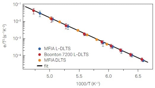
Figure 4. Arrhenius plot used to extract the defect activation enthalpy and apparent capture cross section. Data obtained by L-DLTS transient analysis and DLTS are shown.
To illustrate the motivation for introducing the L-DLTS method, the resolution of a lock-in filter centered at ~ 450 s-1 obtained by evaluating the Equation 2 integral as a function of en has been calculated. The simulated curve is shown in Figure 5 in comparison with the inverted L-DLTS spectrum (shown also in Figure 3 (b)). This obviously proves the higher resolution of L-DLTS with respect to DLTS; taking into account the full width at half maximum as the resolution limit, in the case of L-DLTS, transients with a time constant ratio of ~2 can be distinguished, while a ten-times lower resolution is obtained using DLTS.
Even though it has been established that L-DLTS resolution is an order of magnitude higher than DLTS, L-DLTS needs a higher SNR and an a-priori knowledge of the temperature interval where the capacitance transient takes place as it is based on isothermal measurements. Thus, L-DLTS should generally be used as a refinement of the DLTS characterization.
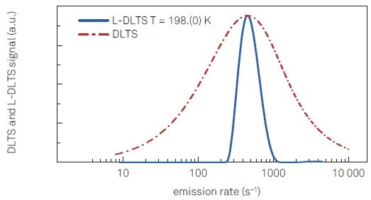
Figure 5. Experimental L-DLTS spectrum extracted from a capacitance transient measured at 198 K (blue trace) and the maximum achievable DLTS resolution calculated for a filtering maximum located at about 450 s-1 (red trace).
Conclusion
DLTS and L-DLTS spectra have been measured on a setup based on a Zurich Instruments MFIA impedance analyzer, and compared to a system using a Boonton 7200 capacitance meter in its highest resolution range. It has been discovered that both systems have similar performance at 1 MHz (the fixed working frequency of the Boonton 7200).
Considering the bigger flexibility of the MFIA instrument in terms of test voltage, frequency and filtering conditions, this makes way to perform DLTS measurements by using the described set-up, thus overcoming the boundaries of the commonly available commercial DLTS and L-DLTS systems such as recovery time, overload and fixed working frequency.
References
[1] J Wei. Deep Level Transient Spectroscopy Using HF2LI Lock-in Amplifier.
[2] K. Goscinski and L. Dobaczewski. Laplace transform transient processor and deep level spectroscopy http://www.laplacedlts.eu.
[3] R. Schifano; E. V. Monakhov; U. Grossner and B. G. Svensson. Electrical characteristics of palladium schottky contacts to hydrogen peroxide treated hydrothermally grown ZnO. Appl. Phys. Lett., 91:133507, 2007.
[4] P. Blood and J. W. Orton. The Electrical Characterization of Semiconductors: Majority Carriers and Electron States. Academic Press, 1992.
[5] For simplicity, the case of a majority carriers trap and n-type semiconductor has been assumed.
[6] The so called dilute limit, Nt << Nd, has to be valid for Equation 1 being fulfilled, as a rule of thumb a Nt / Nd ratio of approximately 10 - 20 percent is generally assumed as upper bound.
[7] L. Dobaczewski; A. R. Peaker; and K. B. Nielsen. Laplace-transform deep-level spectroscopy: the technique and its applications to the study of point defects in semiconductors. J. Appl. Phys., 96:4689, 2004.
[8] F. Schmidt; S. Muller; H. von Wenckstern; G. Benndorf; R. Pickenhain; M. Grundmann. Impact of strain on electronic defects in (Mg, Zn) O thin films. J. Appl. Phys, 116:103703, 2014.

This information has been sourced, reviewed and adapted from materials provided by Zurich Instruments.
For more information on this source, please visit Zurich Instruments.