Authors: Sharang S. TESCAN BRNO s.r.o., Czech Republic, and, Paul Anzalone, TESCAN Group, Warrendale USA
Abstract
The continued downward trend in CMOS feature size has made physical failure analysis an increasingly bigger challenge. In order to fulfill the demand for ever more sophisticated circuit designs and functions, it is imperative to increase the number of transistors and layer stacks. Thus, layer-by-layer deprocessing is becoming increasingly vital, challenging and time consuming for multiple industrial and research applications like physical failure analysis, reverse engineering of the chips, patent violation checks. Ga-FIB is the go-to tool for chip material analysis in the semiconductor industry for applications like TEM lamella preparation, circuit edit, and cross-sectional analysis. We have previously used a Xe plasma FIB successfully for delayering on 14 nm technology from metal 8 to transistor contacts in combination with special chemistry like A-Maze and Nanoflat. Here we show that a gallium FIB with the same chemistry can also perform delayering on a Intel 14 nm technology microprocessor.
Introduction
Strategically removing a set of layers from a packaged chip to isolate a structure of interest is called delayering. It was common practice to employ chemical etching using liquid or plasma chemistry or mechanical means such as polishing off each unwanted layer. It still is a key sample preparation technique in today’s semiconductor industry especially for technology chips of sub-20 nm nature. Several publications reiterate the importance of physical deprocessing to resolve critical yield problems in wafer fabrication, for forensic labs to occasionally reverse engineer chips or to find spyware circuitry altogether making for expansive amounts of work in cyber-security. Mechanical polishing cannot precisely remove layers in a localized manner. Gallium FIB combined with A-Maze or Nanoflat can remove dissimilar materials with very similar material removal rates allowing final RMS of planarity of the exposed layer below 10 nm overall topography.
A multi-million dollar IC design and manufacturing process requires assistance in gallium focused ion beam systems for nodes 28 nm or smaller, and much more than on older nodes. A robust and precise capability was required for lamella preparation (as an aid in fault localization), circuit edit, and qualitative analysis like energy dispersive spectroscopy. Such a complex set of requirements means that FIBs are strategically placed for reducing costs, optimizing performance and functionality, as well as mitigating risks and speeding time to market for complex device designs.
Standard ion-beam sputtering from a gallium FIB with its many benefits often requires the incorporation of special precursors that can help make milling operations smoother by mitigating side effects like re-deposition, and to help overcome or achieve selective etching. A gallium FIB can perform delayering on semiconductor chips for applications like reverse engineering, cyber-security and physical failure analysis for eventual lamella preparation since it enables one to study the unique architectural or material characteristics. It is extremely effective in terms of initial planar removal of multiple layers and subsequent TEM lamella prep in the area of interest. Gallium ion implantation into such samples changes the electrical characteristics like I-V curves. In applications where I-V curves need to maintain their fidelity, Xe+ FIB is used to perform delayering.
Experiment Details and Results
The point of critical interest for gallium FIB based delayering is the same as with Xe+ FIB – the ability to stop the process accurately at any chosen depth in thin sensitive layers of via or metal. It is done in a way that faithfully retains the planarity of the substrate according to the original design. This helps identify faulty design, logic circuitry irregularities in any given layer that can somehow affect intended functionality.
Front-side delayering was performed on an Intel 14 nm processor chip using the flagship S9000G gallium FIB. The top layers of the die were removed using mechanical polishing, exposing a gradient such that the deep underlying layers became accessible. Fig. 1a shows the via contact layer delayered over a 20 x20 µm² area using A-MAZE chemistry using a low beam current and relatively low beam energies. It is clear that dissimilar material has been removed in a planar fashion (Fig. 1b). The process of removing ten layers of metal and via took about 12 minutes under optimized working conditions and a constant gas flux of A-MAZE precursor at the surface.
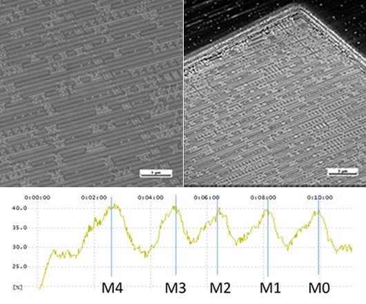
Fig.1a). Delayered Via contact layer (VCx), b). Delayered box of 20 x 20 µm² with smooth polished walls, c). End Point Detection (EPD) curve for monitoring and controlling the delayering process.
The collected and plotted SE signal acts as a control parameter where each peak represents a metal line and every trough represents a via layer (Fig. 1c).
Conclusions
In this paper, the extended capability of a Ga FIB with special gas chemistry is demonstrated by performing delayering on an Intel 14 nm chip. The method delivers significant advantages in terms of localized, precise and layer-by-layer removal along with constant monitoring using the acquired SE signal for end point detection . The process is capable of performing delayering for 10-12 layers on sub-20 nm process nodes. It enhances the workflow capability by enabling the production of ultra-thin lamellae for TEM based analysis making it a ‘must-have’ tool in semiconductor physical failure analysis.
Independent service labs that often provide architectural analyses of microprocessor chips will find this application of vitally important especially for recognising malicious logic gate alterations that can somehow be used in espionage. It can also help uncover patent violation or yield information on faulty design. The extended capabilities of the Ga-FIB will thus make it more important and will continue to play a critical role as an enabler of technological growth in the semiconductor industry.
Acknowledgments: The authors would like to acknowledge funding support from the Technological Agency of the Czech Republic *TE 01020233 (AmiSpec) and also Brenda Prenitzer Ph.D., from Nanospective, Orlando, Florida USA for providing 14nm technology samples for the delayering process.
References
- P. Carleson P et al., “Delayering on Advanced Process Technologies using FIB,” 40th ISTFA Conf. Proc. (2014)
- R. Alvis, et al, “Plasma FIB DualBeam: Delayering for Atomic Force nanoProbing of 14 nm FinFET Devices in an SRAM Array” 41st ISTFA Conf. Proc. (2015)
- J. V. Obona et.al, “Delayering14 nm Node Tech. IC with Xe Plasma FIB” EU. Micro. Cong. Proc (2016)
- V. Viswanathan, Sharang et.al, “Precision Xe Plasma FIB Delayering for Physical Failure Analysis of sub-20 nm Microprocessor Devices” (2017)
TESCAN Group
Founded in 1991 by a group of managers and engineers from Tesla with its electron microscopy history starting in the 1950’s, today TESCAN is a globally renowned supplier of Focused Ion Beam workstations, Scanning Electron Microscopes and Optical Microscopes. TESCAN’s innovative solutions and collaborative nature with its customers have won it a leading position in the world of nano- and microtechnology. The company is proud to participate in premier research projects with prominent institutions across a range of scientific fields. TESCAN provides its clients with leading-class products in terms of value, quality and reliability. TESCAN Group is the North American arm of TESCAN Group, a multinational company established by the merger of Czech company TESCAN, a leading global supplier of SEMs and Focused Ion Beam workstations, and the French company ORSAY PHYSICS, a world leader in customized Focused Ion Beam and Electron Beam technology.

This information has been sourced, reviewed and adapted from materials provided by TESCAN Group.
For more information on this source, please visit TESCAN Group.