The two technologies used to achieve deep etches in the fabrication of micro-electro-mechanical systems (MEMS) are the Bosch process and the Cryogenic Process. Both system and process development over the years have allowed the techniques to advance but the fundamental aspects of each remain the same. In the same timescale we have seen the increasing importance of nanoscale etching for Nano Imprint Lithography, Storage Media etc. Where MEMS structures range in depth from around 10µm up to 500µm with typical openings of >1µm. Although definitions vary nanoscale usually refers to structures below 100nm etched up to several microns deep. It is difficult to use the Bosch process for this type of structure due to the nature of the etching process, cryo etching lends itself to this feature size. We will also describe an alternative process.
The Principle of The Bosch Process
The Bosch process uses a fluorine based plasma chemistry to etch the silicon, combined with a fluorocarbon plasma process to provide sidewall passivation and improved selectivity to masking materials. A complete etch process cycles between etch and deposition steps many times to achieve deep, vertical etch profiles. It relies on the source gases being broken down in a high-density plasma region before reaching the wafer, which has a small but controlled voltage drop from the plasma. This technique cannot be performed in reactive ion etch systems (RIE), as these have the wrong balance of ions to free radical species. This balance can be achieved in high-density plasma systems (HDP). The most widely used form of HDP uses inductive coupling to generate the high-density plasma region so is known as ‘inductively coupled plasma’ (ICP). Sulphur hexafluoride (SF6) is the source gas used to provide the fluorine for silicon etching. This molecule will readily break up in high-density plasma to release free radical fluorine. The sidewall passivation and mask protection is provided by octofluorocyclobutane (c-C4F8), a cyclic fluorocarbon that breaks open to produce CF2 and longer chain radicals in the high-density plasma. These readily deposit as fluorocarbon polymer on the samples being etched. The profile, etch rate and selectivity to the mask material are all controlled by adjusting the etch step efficiency, the deposition step efficiency or the ratio of times of the two steps. The process is relatively insensitive to the exact nature of the photoresist, to the extent that it does not need hard baking of the resist prior to etching. In fact, it is best to avoid high temperature bakes of resist, as this causes variation in the resist profile, which can cause mask recession problems on certain structures.
The Fundamentals of a Good Bosch Etching System
The fundamentals of a good Bosch etching system are described below; There are a number of significant features of the equipment used for Bosch processing which differ from normal ICP systems:
- Fast Pumping
- Fast Response Mass Flow Controllers
- Separation Between Wafer and ICP Region
- Purely Inductive Coupling of Power in the ICP Region
- Heating the Walls, Lid and Pump Lines
- Short Mixed Gas Line
- High Efficiency Wafer Cooling
Fast Pumping
In order to achieve high etch rates, it is necessary to use high flows of process gases. This can only be achieved at the desired pressure by using high efficiency pumping. In general, this means using a larger capacity Turbomolecular pump than would normally be considered necessary for the size of chamber/pressure, and backing this with an appropriate high capacity rotary pump.
Fast Response Mass Flow Controllers
Fast response mass flow controllers are needed for the Bosch Process.
Separation Between Wafer and ICP Region
Minimum 100mm separation between wafer and ICP region. This lowers the ratio of ions to free radicals, as the free radicals have longer decay times than the ions. Both species are needed in the process, but too many ions can result in profile problems, while more free radicals simply increase the silicon etch rate.
Purely Inductive Coupling of Power in the ICP Region
Purely inductive coupling of power in the ICP region. This gives better uniformity of plasma within the ICP region. Capacitive coupling will vary between the driven and grounded parts of the coil, causing differences in ion density. This variation of ion density will affect both the profile uniformity, and can cause contamination effects (such as ‘black silicon’) if there is attack on the ICP tube material.
Heating the Walls, Lid and Pump Lines
The walls, lid and pump lines should be heated. This reduces the deposition of fluorocarbon polymer in regions where it may flake and fall as particles on the wafer. It also minimises the deposition of sulphur compounds in the pumping line and on the turbo pump, which can cause reliability and maintenance problems.
Short Mixed Gas Lines
Short mixed gas line between the mass flow controllers and the process chamber. There will be a time delay between the mass flow controllers opening and the gas reaching the chamber. Keeping the mixed gas line short will minimise this delay, allowing shorter step times.
High Efficiency Wafer Cooling
High efficiency wafer cooling to remove heat from the wafer generated by the use of higher ICP powers and higher etch rates
A typical system layout is shown below:
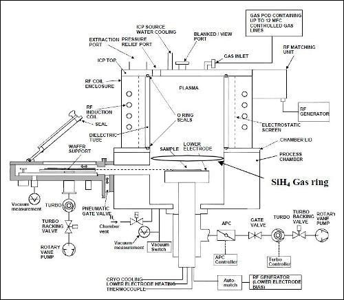
Figure 1.
Advances in The Bosch Process
When the Bosch process was originally introduced for MEM’s applications the highest etch rates of silicon using this technique were in the region of 3-5µm/min. Now claims are made for the Bosch process of etch of more than 50µm/minute. However, these high etch rates are only achievable under some circumstances of very low exposed areas and as the Bosch process uses gas chopping switching between isotropic etch and polymer formation, etching at these rates usually leaves rough sidewalls. It is also well documented that to achieve these high etch rates requires very high gas flows of both SF6 and C4F8 and large turbomolecular pumps, which lead to high costs of ownership. These are not needed as most applications in practical terms (depending on the device requirements of sidewall smoothness etc.), require etch rates only in the range of 5-20µm/min, and even lower etch rates are required to produce smooth sidewalls for optical applications. In practice, to achieve the majority of device needs, the process requires precise gas control and switching, quick RF matching and fast response pressure control which are not possible to achieve at higher etch rates.
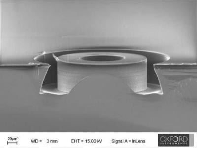
Figure 2 shows a typical result from a bulk silicon etch. This process was performed on a 150mm wafer with patterned resist over about 30% of the wafer. This etched at a rate of 17microns/minute with a near vertical profile. The higher rates are usually achieved by higher ICP powers with higher etch time compared to polymer time which can lead to some sidewall breakdown due to the polymer film not forming a complete coverage of the silicon sidewall. Etch uniformity across the wafer was ±3%.
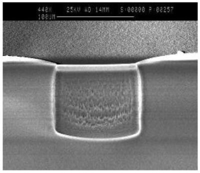
Figure 2. 100µm deep etch at 17µm/min
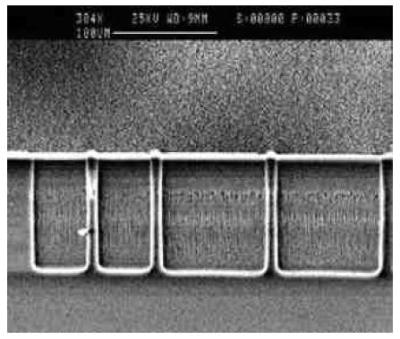
Figure 3. 110 µm deep etch
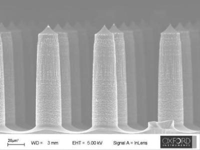
Figure 3 shows a bulk etch process etched at a slower rate of 10µm per minute with vertical sidewalls. By controlling the gas switching ratios, pressure and power, high rate processing up to 10µm/min through wafer etches can be achieved with smooth sidewalls as shown in figures 4a-c, even at 10:1 or greater aspect ratios
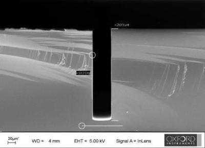
Figure 4a. Through wafer etch with smooth sidewalls
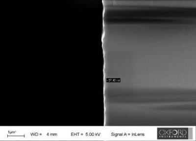
Figure 4b. Sidewall roughness
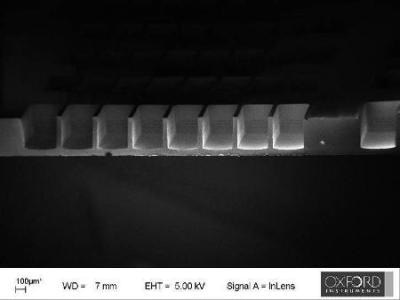
Figure 4C. Through wafer etch
Aspect Ratio Dependent Etching (ARDE)
This problem arises when there is a range of different size trenches on one wafer, which will reach differing depths in a given time. This is clearly seen in Figure 5. This effect is geometrical, being more severe for vias than for trenches. In the past this could only be optimised if etching to a buried oxide layer or SOI layer but now by controlling the deposition cycle of the process ARDE can either be reduced or eliminated as shown in Figure 6 which shows trenches etching at similar rates to large open areas etching.
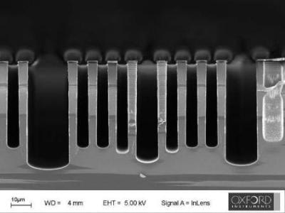
Figure 5. Trench depth variation with width
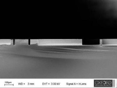
Figure 6. Control of ARDE
Etching Down to a Buried Oxide Layer
Etching down to a buried oxide layer has its own hazards. The biggest difficulty is in controlling the behaviour of the process once it hits the buried layer. If the process is simply left on to achieve a timed over-etch period, this will cause ‘notching’, see Figure7. This is a continuing etch into the oxide at the corners of the etched feature. This is partly caused by charging of the buried oxide. This pushes the ions into the corners of the etched features, removing sidewall protection in that area. This allows attack by the etchant species, causing lateral etching. This can be controlled by controlling the ion energy by reducing the RF power as the etch reaches the interface in combination with the gas ratios. The technique most frequently adopted to eliminate is to actually pulse the platen power at a predetermined frequency. This reduces the charge build up at the SOI interface and thus reduces the notching at the interface - this can be seen in Figure 8. The amount of notching versus duty cycle is shown in figure 9 for different trench sizes.
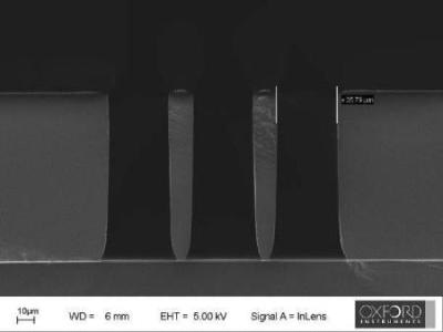
Figure 7. Notching at buried oxide interface
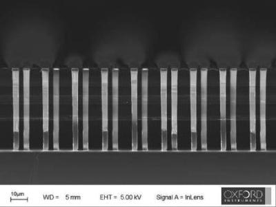
Figure 8. Control of Notching at SOI interface using RF Pulsing
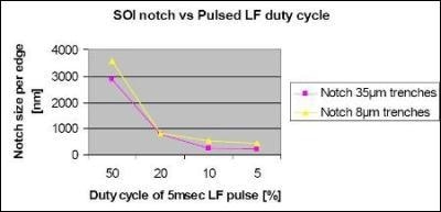
Figure 9. Graph showing SOI notch control vs. Duty Cycle
Application of The Bosch Process
Typical Application of the Bosch process are highlighted below:
- MEMS
- Microfluidics
- Medical
MEMS
Microfluidics
Medical
Summary
The Bosch process offers higher etch rates but at the cost of sidewall roughness. To limit this roughness the rates are usually in the region of 10-20µm, which is still higher then the cryo process. To achieve the ultra high etch rates claimed for the Bosch process means very high flows of gas and requires very big turbomolecular pumps, which result in a higher cost of ownership. The Bosch process also does not offer very good positive profiles, which the Cryo can. The cryo process has also found a growing market in the etching of Nanostructures as the Bosch process leaves scallops in the walls, which in most case is undesirable for the application.
Both the Bosch process and Cryo process will find use in the growing field of integrated sensors and actuators, but Cryo has distinct advantages in the nanoscale arena. In the end, the user must decide which process will be most appropriate for their application.

This information has been sourced, reviewed and adapted from materials provided by Oxford Instruments Plasma Technology.
For more information on this source, please visit Oxford Instruments Plasma Technology.