In recent years, STEM-in-SEM (the industry acronym for Scanning Transmission Electron Microscopy in an SEM) has increased in popularity for a number of experts. This technique has drawn attention from a diversity of scientific professionals, including biologists, polymer scientists and materials scientists, thanks to its cost-effectiveness, ease of use and high resolution.
STEM-in-SEM is particularly suited to investigations into the internal structure of thin-film (100-200 nm) samples, in addition to the shape and size of submicron to nanometer particles. In part due to the beam-sample interactions, there are limitations in the ultimate resolution that can be achieved with standard SEM imaging modes on bulk samples.
The sample is very thin, and interaction volume is particularly small with STEM-in-SEM. This, therefore, means that the resolution more closely approximates the diameter of the electron beam at the exit surface of the sample, which therefore permits high resolution; sub-nanometer resolution is easily achieved through the use of STEM with JEOL’s state of the art FE SEMs.
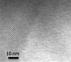
STEM-in-SEM image of Faujasite zeolite with 7.4 A lattice spacing. Image Credit: JEOL USA, Inc.
Often, the method of STEM-in-SEM is termed a ‘low voltage STEM’ technique. The use of the term ‘low voltage’ refers to the typical operating energies of 20-30 kV, which are used in the SEM, as opposed to the more conventional 100-300 kV that are used with a traditional dedicated STEM or TEM.
There are advantages of low voltage STEM, even though it admittedly cannot compete with the results offered by dedicated STEM or TEM. Particularly for low atomic number components or low-density specimens, using accelerating voltages of 30 kV or lower enhances image contrast. This enhanced image contrast at lower voltages means that STEM-in-SEM is an ideal method when characterizing biological samples.
Some of STEM-in-SEM’s alternative advantages include reduced risk of potential sample damage, reduced charging, and reduced contamination.
Traditionally, there are two configurations that are used for STEM-in-SEM method: the first of these is a STEM converter and the second a dedicated STEM detector. The STEM converter provides a simple and cost-effective method for obtaining a bright-field STEM image; it fits in an SEM just as a standard sample holder would without requiring an additional detector or hardware.
A STEM converter has a hole through it and holds a 3 mm diameter sample (approximately the typical size for TEM/STEM holders). The sample is scanned by the beam, and transmitted electrons transmit to a polished mirror surface below the sample. These electrons are then converted into secondary electrons, which are themselves detected by the in-chamber secondary electron detector.
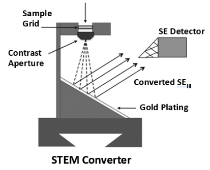
Image Credit: JEOL USA, Inc.
It is easy to interface STEM detectors with SEMs, and ultrathin sections or nanometer range particles that are mounted on grids can then be monitored using the same optics as a regular SEM operation. More flexibility is facilitated by a dedicated STEM detector, such as both bright-field and darkfield STEM imaging or the utilization of a multi-grid holder for higher throughput.
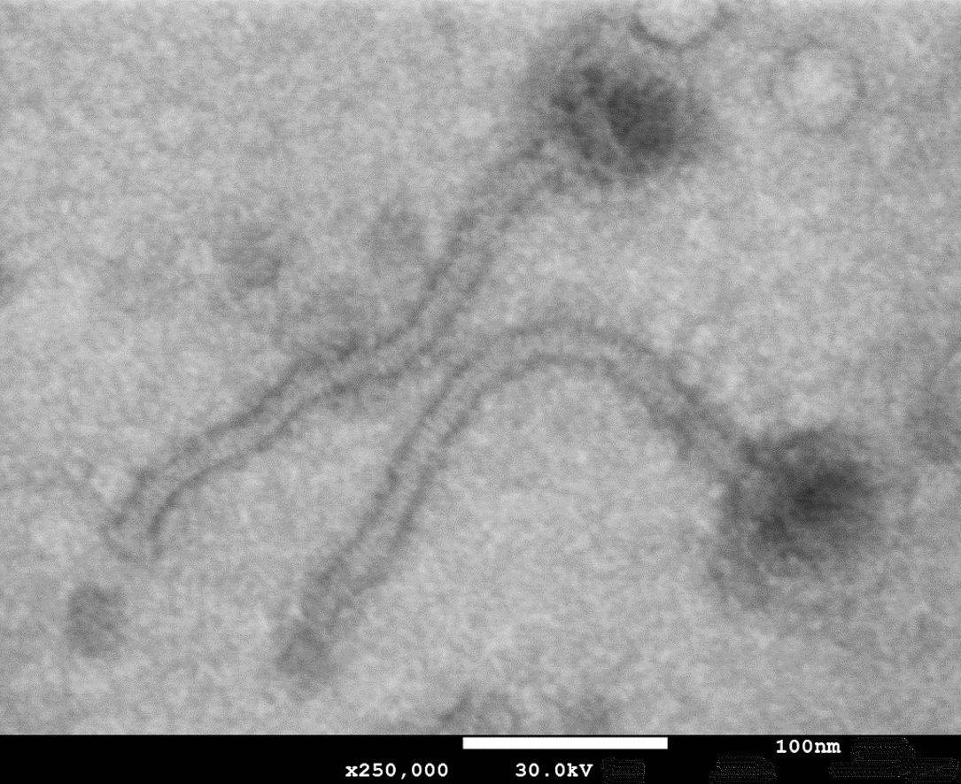
Image Credit: JEOL USA, Inc.
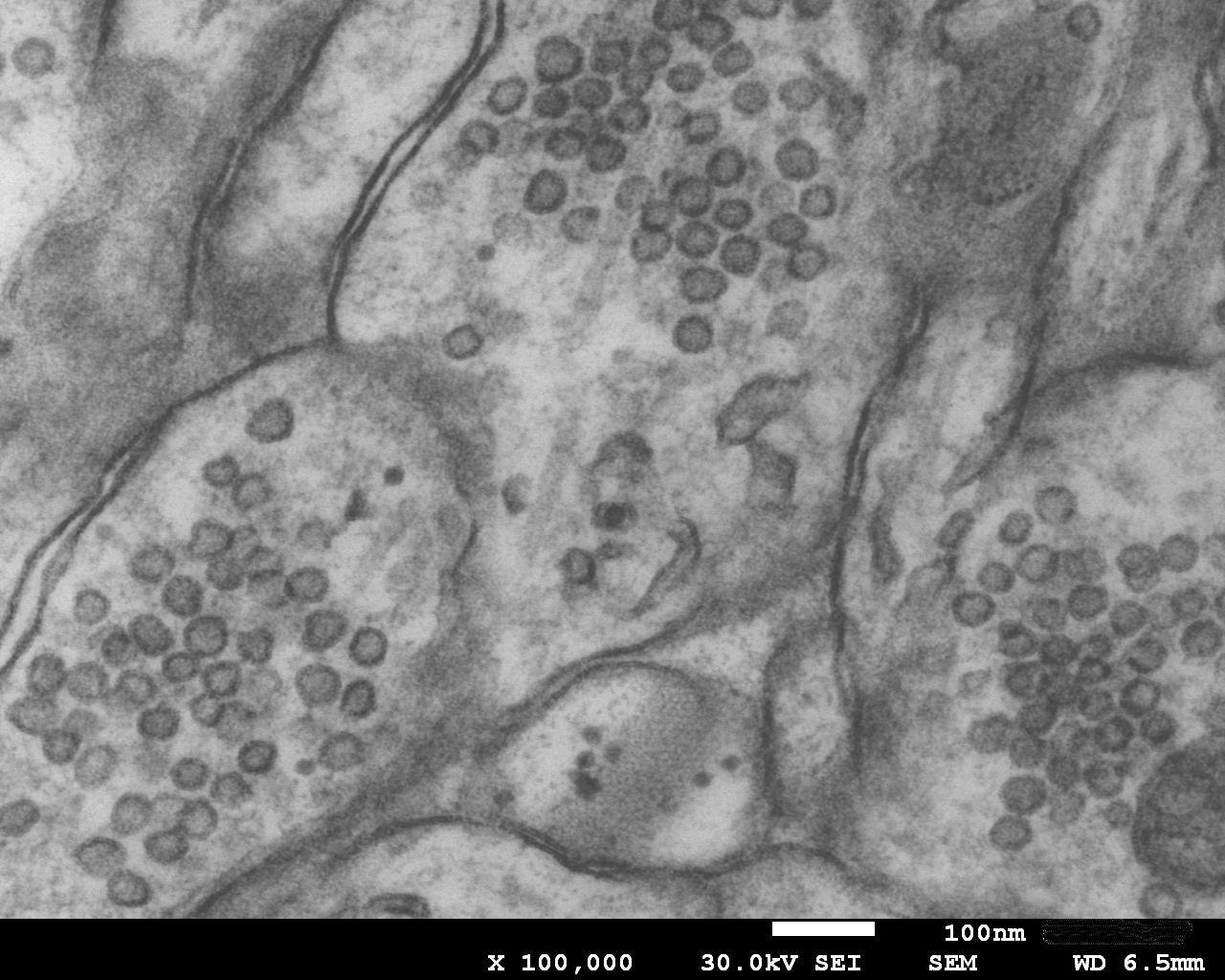
Image Credit: JEOL USA, Inc.
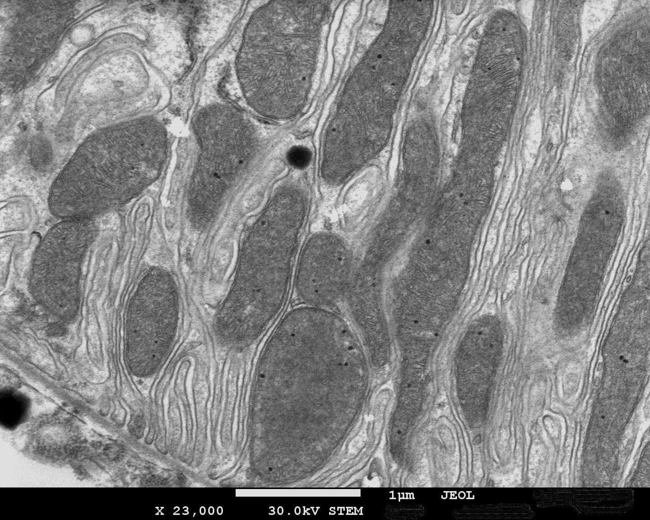
Image Credit: JEOL USA, Inc.

This information has been sourced, reviewed and adapted from materials provided by JEOL USA, Inc.
For more information on this source, please visit JEOL USA, Inc.