The new JEOL JEM-ARM300F2 Grand ARM™2 is engineered for ultrahigh-resolution imaging at the picometer scale, combining this precision with highly sensitive EDX and high-resolution EELS analysis across a wide range of accelerating voltages. The GRAND ARM2 enables detailed atomic-level characterization for a broad spectrum of materials.
At the heart of the system is a newly designed objective lens pole piece. This small-gap lens, optimized for peak resolution, supports configuration with dual large-area (158 mm2) Silicon Drift Detectors (SDDs), achieving a combined EDX solid angle with Ni P/B ratios exceeding 4000.
This design delivers both exceptional TEM/STEM resolution and enhanced EDX sensitivity. EELS performance is also advanced, with optimized data acquisition extending beyond 5,000 eV.
Ease of use is built in through automated accelerating voltage settings, Cs corrector alignment routines, and lens optimization procedures - making the GRAND ARM2 not only a high-performance instrument, but also a practical one for advanced atomic-scale imaging and analysis.
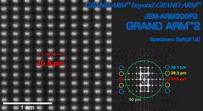
Image Credit: JEOL USA, Inc.
No Compromise in Spatial Resolution
New pole piece design yields increased EDS solid angle without sacrificing resolution.
Mitigation of Environmental Effects
New enclosure reduces impact of air flow, temperature changes, and acoustic noise.
Ultimate Functionality
Automated HT settings, corrector alignments, and optimized lens routines promote ease of use.