The small but mighty semiconductor has become an integral part of our high-tech world. Popularly known as microchips or integrated circuits (ICs), semiconductors are employed in a constantly increasing number of commercial, industrial and consumer products. A very short sampling of semiconductor uses involves:
- Personal electronic devices, for example, smart watches, computers and tablets and mobile phones
- Household products such as appliances, LED light bulbs, heating/cooling equipment and televisions
- Industrial and commercial products such as optical sensors, lasers, medical diagnostic equipment, solar batteries, industrial machinery and traffic lights
Products purchased by customers drive the majority of semiconductor demand as demonstrated in Table 1.
Table 1. Percent of Semiconductor Demand by End Use, 20191. Source: PerkinElmer
| |
|
| Communications |
33.0% |
| PC/Computer |
28.5% |
| Industrial |
11.9% |
| Consumer Electronics |
13.3% |
| Automotive |
12.2% |
| Government |
1.3% (includes military) |
A common factor is shared by all of these different semiconductor applications: the requirement for electrical properties determined by the application. A semiconductor is a material that has an intermediate amount of electrical conductivity, hence the “semi” prefix.
The material comprises either a single element, normally silicon, or a mixture of elements, for example, indium phosphide (InP), gallium arsenide (GaAs) and a number of others.
The element silicon is the substance most commonly utilized in semiconductors. Silicon is an abundant resource as it is found in one-quarter of the Earth’s crust.
It is found in rock, soil and sand in compound with aluminum, magnesium and oxygen. The silicon must be extracted from the compounds and purified to 99.999999999% for production use.
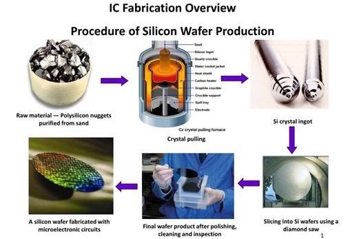
Figure 1. IC fabrication from silicon sand to ingots to wafers with circuitry. Image Credit: PerkinElmer
The conductivity of the material can be modified by adding small amounts of impurities. The term for this process is “doping,” and it can significantly increase the conductivity of the semiconductor.
The conductivity of silicon also changes according to the ambient temperature, with higher conductivity resulting from higher temperatures.
The huge variety of semiconductor end uses nods to the enormous influence that the industry has on the global economy. In 2019, global semiconductor sales reached USD $412.3 billion. In 2020, international semiconductor industry sales were forecast to reach USD $433 billion.1
Worldwide semiconductor sales were USD $34.4 billion for April 2020, a 1.2 percent decline from sales in March 2020, but a 6.1 percent increase across sales in April 2019. These early 2020 sales suggest minimal impact so far from the novel coronavirus pandemic.2
The buyers of semiconductors for the manufacturing of electronic equipment are found across the globe, with the greatest share purchased in the Asia Pacific region:1
- Asia Pacific 62.5% (China 35.0%)
- Americas 19.1%
- Europe 9.7%
- Japan 8.7%
Semiconductor Production
Fabrication and design are the two main phases of semiconductor production.
Fabless firms is the term used for companies that only focus on design. Companies that solely focus on fabrication are known as foundries. Integrated Device Manufacturers (IDMs) are companies that specialize in both design and fabrication.
A summary of the semiconductor production process includes:
Raw Material Processing
- Extraction of silicon from the raw material
- Purification
- Formation of cylindrical ingots, from one to almost 18 inches (450 mm) in diameter, up to 200 pounds each
Research and Development (R&D)
- Process engineering
- Semiconductor design
- Selection of raw and fabrication materials
- Design of Quality Control (QC) program
Blank Wafer Production
Wafer Processing
Wafer Cutting
These primary processes are comprised of 400 to 600 intricate steps that are normally finished in one to two months.
Challenges
The semiconductor industry has particular demands and faces distinct challenges for efficient and successful production.
Detecting Ultra-trace Impurity Levels
Consumers continue to influence the demand for electronic devices that are lighter and smaller without impacting reliability or speed. This demand creates an equivalent need for lighter and smaller semiconductors that are reliable and fast.
The problem that fabricators face is that the smaller the semiconductor, the more exposed it is to interference by particulate and chemical contaminants. Semiconductor manufacturers require the ability to detect ultra-trace levels of contaminants during the process of fabrication.
It is no longer sufficient to detect chemical contaminants at the parts per trillion (ppt) level — parts per quadrillion (ppq) detection limits must now be attained. The detection of particulates must reach nanoparticle size or less.
The purity levels needed for each material utilized in wafer packaging and fabrication must be defined by the R&D team:
- Supplied blank wafers and silicon ingots
- Fine chemicals, for example, bases, solvents and acids
- Ultrapure water
- Specialty and inert gases
- Packaging materials, for example, resins, polymers, solder, dyes, die attachment materials and molding compounds
- Circuit-building materials such as CMP slurry, sputter target and photoresist material
R&D finds the analytical instruments that can attain the ultra-low detection limits required for the possible impurities of each material. Analysis and sampling workflows are tested and developed. Once approved, these are deployed for in-process testing and materials receiving.
Maintaining Production Efficiency
There are several opportunities for physical defects or contaminants to come into contact with the wafers as they travel through the process of fabrication. These issues can make production less efficient or, even worse, can result in product failure or production delays.
It is vital that an extensive process QC program can be created, deployed and maintained. The aim of the program is to identify any issues as early in the workflow as possible to avoid wasted materials and time downstream from the problem.
The R&D team defines the standards of the downstream process and includes them in the design of the production workflow. The process control manager works with the R&D team throughout the design stage and then carries out and observes the QC program.
Important monitoring points, parameters and materials in the production process are:
Blank Wafer Production
- Identify residual particulates and physical deformities after disc polishing and ingot slicing
Clean Room Air
-
Airborne molecular contaminants (AMCs), for example, semi-volatile and volatile organic compounds (SVOCs, VOCs), acids and bases, anions and metals
- Air quality parameters such as humidity and temperature
- Airborne particulates
Ultrapure Water
-
Contaminants such as cations and anions, VOCs and SVOCs, silicates, metals, total organic carbon (TOC) and metals
Circuit Formation Materials
In-process QC monitoring must be almost continual and offer the real-time identification of specification or contaminant failures to be completely effective in maintaining production efficiency.
Error rates as a result of manual sampling can be reduced by a high degree of automation, and integrating the monitoring network online allows for prompt data reporting and an efficient turnaround.
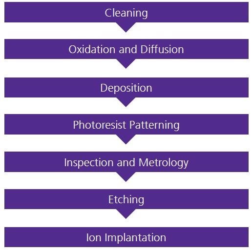
Figure 2. Steps of the circuit formation process are repeated to build a multi-layered IC. Image Credit: PerkinElmer
Regulatory Compliance
Semiconductor manufacturers must uphold compliance with local, state and national regulatory requirements. A selection of almost universal compliance requirements are outlined here.
Permitting
A permit from national, state and/or local regulatory agencies is required by facilities that employ materials that are classed as hazardous in order to store, obtain and use these materials.
The permit outlines the amounts and types of materials that the facility can store, obtain and use in its processes. It also stipulates the record-keeping, reporting and monitoring guidelines to keep the permit.
For semiconductor production operations, air permitting is also a necessity. The permit requirements will be reliant on the facility’s location and the content of the air emissions.
Air permits define the reporting, monitoring and record-keeping requirements to sustain the permit.
Employee Health and Safety
In semiconductor production, some of the chemicals employed have the ability to release particulate matter, VOCs and SVOCs into the indoor air of the facility.
Monitoring programs and exposure prevention protocols are required by fabricators to ensure compliance with regulatory standards that are created to protect the health of employees.
Some of the elements of a successful health and safety program are:
- Target parameters to be monitored
- Personal protective equipment (PPE) requirements
- Analytical sensitivity requirements
- Analysis and sampling schedule and SOPs
- Regulatory reporting guidelines, schedule and means
- Remedial action alternatives
- Record-keeping procedures
- Further regulatory-specific requirements
A well-designed, extensive health and safety program increases employee health and safety and allows the facility to avoid expensive regulatory penalties.
Waste Management
All kinds of manufacturing facilities create process wastewater and additional process wastes. The processes and materials utilized at the facility define the contents of these and other waste streams created by semiconductor fabricators.
A permit and periodic analysis and sampling are required to discharge process wastewater to a treatment facility. The treatment facility will define the standards for reporting, testing and content restrictions.
Alternative process wastes can include contaminated or off-specification materials. Characterization, transport and storage of the wastes should adhere to national, state and local requirements.
If any wastes are classed as hazardous, a special permit may be required.
The waste treatment or disposal facility will need analytical data regarding the content of each individual waste stream to make sure that their acceptance of the waste is compliant with the requirements of its operating permit.
Minimizing Environmental Impacts
As with all manufacturers, semiconductor producers must evaluate the environmental consequences of their operations.
Considering the environmental impact of a facility can increase the sustainability of an operation, help control costs and meet the regulatory standards for waste disposal and emissions.
To help a facility achieve these goals, a few practical steps are:
- Optimizing process controls to decrease air emissions and the generation of waste. This can also enhance production efficiency and manage costs.
- Utilizing R&D processes to reduce the use of possibly toxic materials in the production process and the end product. This can decrease waste disposal costs and the requirement for additional permits or constrictive permit rules.
- Employing R&D efforts to enhance the recyclability of components in electronic waste. This can increase operational sustainability.
Depending on the amount of external storage or operations at the facility, a stormwater pollution prevention plan may be needed. The plan involves analysis and sampling procedures for stormwater discharges, record-keeping and reporting guidelines and remedial action plans.
Trends
There are many trends evolving in semiconductor production, design and use. Some are quickly advancing, and others have been developing more gradually. Some of the more frequently discussed trends are outlined here.
Smaller ICs
R&D developments continue at a rapid speed to further decrease the size of semiconductors.
The industry has advanced from the 10 μm technology of the early 1970s to the modern-day 7 nm chips, and industry leaders aim to produce even smaller chips: 5 nm, 3 nm and smaller.
At present, 7 nm ICs are predominantly used, 5 nm ICs are in production, and 3 nm ICs are in development.
Two main priorities for 3 nm and smaller chips are to decrease energy use while increasing performance. R&D teams are striving to achieve these goals, in part, by moving from finFET to GAAFET technology.
As chips reduce to 3 nm and smaller sizes, fabricators will also require novel methodologies and equipment for deposition, lithography, QC analytics and etching.3,4
Fabless Designers and Independent Foundries
The movement toward more fabless chip design companies is continual, and a growing amount of technology businesses are producing their own chips in-house.
These trends are influenced by the growing demand for more tailored chips that are specific to the application, engineered to optimize the algorithms and software specific to the business.
The demand for and success of independent semiconductor foundries is being driven by the fabless design-only and in-house design trends.
Worldwide expenditures for new foundries are predicted to be USD 50 billion in the next few years. It will be interesting to see how much of the foundry growth is invested in independent foundries.5,6,7
Artificial Intelligence (AI)
The amount of data processed by AI systems continues to increase rapidly. Novel algorithmic-specific chips continue to be developed by the semiconductor industry to offer the processing speed required for AI data.
Internet of Things (IoT)
IoT systems create enormous amounts of data that is employed to make decisions in real-time.
The semiconductor industry continues to expand its R&D of new chip materials, silicon photonics and materials that will improve the stability and processing capabilities of IoT data.
Autonomous Vehicles (AVs)
Semiconductors will continue to be a major influence in the effective development of fully autonomous vehicles.
References and Further Reading
- Semiconductor Industry Association (SIA). 2020a. 2020 Factbook. https://www.semiconductors.org/resources/factbook/.
- SIA. 2020b. https://www.semiconductors.org/. June 1.
- Semiconductor Engineering. 2020. Making Chips at 3 nm and Beyond. https://semiengineering.com/. April 16.
- Tom’s Hardware. 2020. Samsung Prototypes First Ever 3 nm GAAFET Semiconductor. https://www.tomshardware.com/news/samsung-prototypes-first-ever-3nm-gaafet-semiconductor. January 3.
- Cole Reports. 2020. Semiconductor Foundry Market to Witness the Highest Growth Globally in Coming Years 2020- 2026. https://coleofduty.com/news/2020/05/13/semiconductorfoundry-market-to-witness-the-highest-growth-globally-incoming-years-2020-2026/. May 13.
- Semiconductor Digest. 2020. Technology Trends in Semiconductors Revealed by GlobalData. https://www.semiconductor-digest.com/. February 10.
- TechNewsWorld. 2019. Structural Shifts in Semiconductor Industry Spawn New Trends. https://www.technewsworld.com/. March 8.

This information has been sourced, reviewed and adapted from materials provided by PerkinElmer.
For more information on this source, please visit PerkinElmer.