In recent decades, the Field Emission Scanning Electron Microscope (FE-SEM) has become a cornerstone of analytical science, offering professionals across various scientific and engineering disciplines numerous advantages over conventional SEMs.
This technology facilitates a deeper understanding of complex processes and emerging technologies.
This article discusses this innovative technology and Hitachi’s range of FE-SEM microscopes.
Field Emission Scanning Electron Microscope
The most common electron sources for an SEM include Tungsten (thermionic), Schottky and Cold Field Emission (CFE) sources. An FE-SEM is defined as a SEM equipped with a field emission gun. These microscopes currently provide superior performance in terms of resolution, detection strategies, analytical capabilities, and beam stability.
Hitachi is the only company in the market that offers SEMs with both Cold Field and Schottky Emitters.
Benefits of the SU8600 Microscope Range
The SU8600 represents Hitachi's latest Cold Field Emission SEM, integrating advanced imaging modes with three in-lens detectors and Energy Dispersive X-ray (EDX) detectors, achieving a lateral resolution as fine as 10 nm.
All users of the SU8600 can leverage Hitachi’s extensive experience in manufacturing FE-SEMs, which dates back to the introduction of the first CFE-SEM in 1972. In 2012, Hitachi received the esteemed IEEE award for its ongoing innovations in this domain, with over 9,000 units installed worldwide.
Benefits for Academia and Industry
Maintenance costs and equipment availability are critical concerns for both industry and academia. A cold field emission source's theoretical unlimited lifetime minimizes downtime associated with tip exchanges in an SU8600. Many users of CFE SEMs have not replaced their emitters for over fifteen years, resulting in significant long-term savings.
Many customers utilize the SU8600 as a 30 kV Transmission Electron Microscope, combining the advantages of a SEM, particularly through-the-lens detection with those of a TEM.
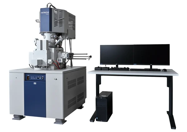
Image Credit: Hitachi High-Tech Europe
Comparison with Competitors
In terms of benefits, such as exceptional imaging performance, extended tip life, and low emission currents starting at 1 µA, there are currently no competitive models in the market.
However, specific applications may have unique requirements, such as higher currents, a pull-out chamber door, or a Variable Pressure mode to accommodate a broader and potentially diverse range of samples. For certain applications, a Schottky Emitter may be a more suitable option.
With the introduction of the SU8600 and SU8700, Hitachi now offers two FE-SEMs that share the same operational, software, and automation features but possess distinct electron optics, each with its own unique advantages.
Benefits of the SU8700
Hitachi’s FE-SEM product line, the SU8700 and SU7000 serve as versatile solutions. They provide exceptional flexibility in imaging and vacuum modes, requiring chambers equipped with multiple ports for accessories and stable currents of up to 200 nA.
The SU8700 Microscope series is advantageous for all sectors and industries that demand high flexibility to address challenges in failure analysis and process control efficiently. Notably, it is beneficial in the chemical industry, where product cycles are short and material changes occur frequently, as well as in the semiconductor industry.
Advice for Businesses
Hitachi encourages businesses to contact them to submit a sample. Based on the specific requirements and needs, Hitachi can recommend the microscope from their extensive range that best suits the application.
Tip of the Month
To achieve high-resolution images at magnifications exceeding 20,000x, avoid using double-sided carbon tapes for securing bulk samples.

This information has been sourced, reviewed and adapted from materials provided by Hitachi High-Tech Europe.
For more information on this source, please visit Hitachi High-Tech Europe.