The technique of Cathodoluminescence (CL) is widely employed in electron microscopy. It is routinely applied across various geological studies, including defect states and dating; materials science to provide insights into the photonic properties of semiconductors, such as solar cells; and pharmaceuticals to analyze the distribution of active pharmaceutical ingredients.
This article examines how CL investigations can be efficiently and effectively conducted using Hitachi’s TM4000Plus benchtop SEM.
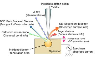
CL is one of several processes that occur when an energetic electron beam interacts with a sample. Typically, SEM utilizes electron signals such as secondary electrons (SE) for topographical imaging and backscattered electrons (BSE) for compositional imaging.
In addition to these electron signals, a spectrum of electromagnetic radiation is generated, including X-rays used for elemental analysis (EDX/EDS).
Certain materials can also emit photons in the infrared, visible, and ultraviolet wavelengths. These photons can provide valuable information regarding subtle compositional variations, bandgap, chemical bonding, crystal structure and defects.

Figure 1. Typical interactions and signals in SEM. Image Credit: Hitachi High-Tech Europe
Traditionally, CL imaging is performed by incorporating a dedicated photon detector into an SEM. This detector captures photons instead of electrons and may be panchromatic (detecting a wide range of wavelengths) or monochromatic (detecting specific wavelengths as needed).
It may consist of a simple light guide and photomultiplier tube positioned near the specimen.
To enhance collection efficiency, the detector may also feature a parabolic mirror positioned above the specimen. This mirror can be connected to a photomultiplier tube or a spectrometer for spectral analysis of photon wavelengths.
However, the Hitachi TM4000Plus enables the identification of panchromatic CL without any adjustments. This capability facilitates numerous panchromatic CL investigations straightforwardly and cost-effectively using a readily available instrument.
The TM4000Plus includes a low vacuum secondary electron detector (designated as UVD) based on light collection technology, allowing CL detection to be initiated with the press of a button.
The bias typically applied to enhance secondary electron detection is disabled, enabling the detector to function as a photon detector, with the secondary electron signal suppressed.
Additionally, the TM4000Plus features a high-performance backscattered electron detector and dual-channel image handling capability, allowing for the concurrent acquisition of compositional and CL information (as demonstrated in the example in Figure 2).
The datasets can be further enhanced if the optional EDX elemental mapping capability is utilized, providing qualitative and quantitative chemical information promptly.

Figure 2. Zonation study in coarse grained syenite with alkali feldspar. From left – CL image showing zonation, BSE image showing composition contrast and Mixed (CL + BSE) image recorded simultaneously. Image Credit: Hitachi High-Tech Europe
CL Imaging in Materials Science
In materials science, CL imaging is a powerful technique for elucidating the crystallographic properties or bonding states of materials. In Figure 3, a multi-phase TiO2 sample was analyzed.
The backscattered electron image (left) shows no significant contrast variation due to the specimen's uniform compositional characteristics.
However, the CL image (right) reveals distinct regions corresponding to the rutile and anatase phases of TiO2. The CL detector in the TM4000Plus is particularly sensitive in the shorter wavelength range, resulting in the anatase phase appearing bright, while the rutile phase (where emitted photons have a wavelength greater than 500 nm) appears dark.
This prompt and straightforward method eliminates the need for separate spectrophotometric or diffraction studies. It provides spatially resolved information at the sub-micrometer scale, which is challenging to achieve with alternative techniques.

Image Credit: Hitachi High-Tech Europe
CL Imaging in Pharmaceuticals
In pharmaceutical drug delivery systems, such as tablets, the precise distribution of the Active Pharmaceutical Ingredient (API) is essential. The particle size and distribution of the API must be meticulously controlled to ensure efficient uptake in the body. Figure 4 shows an example of a cross-section of a commercial ibuprofen tablet.
The secondary electron image (left) illustrates the roughness associated with the fracture of the tablet. The backscatter electron image (center) displays the enteric (gastric-resistant) coating surrounding the tablet.
The CL image (right), however, provides comprehensive information about the distribution of the API, which can be utilized for both rapid process control and quality assurance.

Image Credit: Hitachi High-Tech Europe
CL Imaging in Geology
CL is extensively employed in geology to investigate subtle variations in crystal formation that may not be discernible through secondary electron imaging, backscatter electron imaging, or energy-dispersive X-ray analysis.
In the example of syenite shown in Figure 5, the BSE image (middle) shows no brightness variation across the crystal due to minimal compositional change. In contrast, the CL image reveals significant brightness variation across the crystal due to zonation.
Another application of this technique is in supporting geological dating of zircons. Variations in U-Th-Pb ratios within zircon crystals can be used to determine the date of crystal formation. The minor variation in U-Th-Pb ratios is often too small to be reliably detected using chemical techniques in the SEM, such as EDX.
Mass spectrometry accurately determines the exact ratios. However, it does not quickly identify areas of interest for examination, creating a challenge.
In this context, CL imaging in SEM can significantly help pinpoint areas of interest for further analysis, substantially accelerating the dating process. The “zoning” evident in CL images of zircons indicates which grains exhibit the largest variations in U-Th-Pb ratios, guiding geologists to focus mass spectrometry on the most relevant crystals.
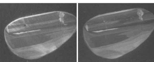
In the example presented in Figure 5, a zircon imaged in conventional SEM with a dedicated CL detector (right) is compared with CL imaging of the same crystal in the TM4000Plus (left). The comparable information obtained from both approaches enables the selection of the most suitable grains for subsequent mass spectrometry.

Figure 3. Zircon grains imaged using the Hitachi TM4000Plus (left) and pan-chromatic CL detector in conventional SEM (right). Image Credit: Hitachi High-Tech Europe
Conclusions
Panchromatic imaging capability can be effectively performed using a Hitachi benchtop SEM to better understand a wide range of material systems.
The ability to overlay BSE and CL data in a single image provides users with precise correlations of chemical and crystallographic or bonding information, whether for standalone studies or to support additional investigations such as subsequent spectrometry or diffraction studies.
These instruments require a relatively small capital investment and laboratory space, offer faster time-to-data, and can be operated with ease by personnel regardless of prior electron microscope experience.
Consequently, they present opportunities for CL studies to be applied more broadly than before, making the capabilities of CL accessible in numerous laboratories, including those focused on process and quality control, as well as in academic settings.
Furthermore, Hitachi benchtop SEMs enable this type of CL work without requiring adjustments or additional hardware investments. When combined with secondary electron (SE) and backscatter electron (BSE) imaging, along with EDX elemental analysis and mapping, these instruments provide a powerful addition to pharmaceutical laboratories, geoscience labs and a diverse array of materials science labs.

This information has been sourced, reviewed and adapted from materials provided by Hitachi High-Tech Europe.
For more information on this source, please visit Hitachi High-Tech Europe.