Sponsored by Park SystemsReviewed by Olivia FrostJun 11 2025
Understanding failure modes, mechanisms, and root causes is critical in the manufacturing of semiconductors and electronic devices. Identifying the underlying cause of a failure not only helps prevent recurrence but also leads to higher product quality, reduced costs, and increased customer satisfaction.
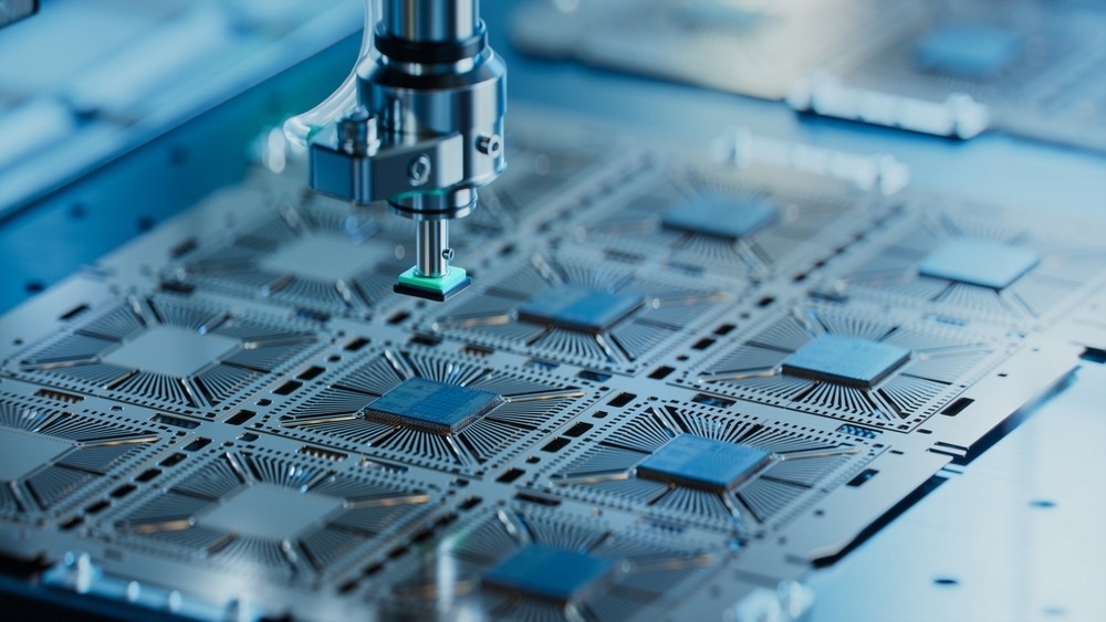
Image Credit: IM Imagery/Shutterstock.com
In the semiconductor industry, failure analysis plays a key role at various stages, from inspecting local defects on bare wafers to evaluating process quality across multiple steps, and assessing the function and performance of finished devices.
As key functional components continue to shrink, failure analysis has become increasingly complex due to the miniature size and intricate architecture of micro- and nano-scale devices. This growing challenge underscores the need for a powerful yet user-friendly tool capable of inspecting, isolating, and characterizing defects with precision.
This article will explore various aspects of failure analysis methodologies in semiconductor and electronic device manufacturing, with a particular focus on the application of atomic force microscopy (AFM) as a versatile and effective tool in this field.
 Download the full version now to read more!
This information has been sourced, reviewed and adapted from materials provided by Park Systems.
For more information on this source, please visit Park Systems.