In this interview, Arash Mirhamed, lead of the ISE Support Team at Park Systems, explores how imaging spectroscopic ellipsometry differs from conventional spot-based methods, where traditional approaches fall short, and why spatially resolved n/k extraction is increasingly critical for advanced materials.
What is imaging spectroscopic ellipsometry, and how does it differ from conventional ellipsometry?
Imaging spectroscopic ellipsometry (ISE) is an optical thin-film characterization technique that combines ellipsometry, spectroscopy, and microscopy. Like conventional spectroscopic ellipsometry, it measures changes in the polarization state of light upon reflection to determine film thickness and optical constants (n and k) over a range of wavelengths.
The key difference lies in the spatial dimension. Conventional ellipsometry measures a single spot and provides averaged parameters over that beam area. It assumes the sample is laterally uniform within the spot.
In contrast, ISE records ellipsometric images comparable to a microscope, meaning that each pixel contains spectroscopic polarization information. This enables the extraction of spatially resolved maps of thickness and optical constants across the field of view. In other words, it carries out spectroscopic ellipsometry on each pixel of the microscope image.
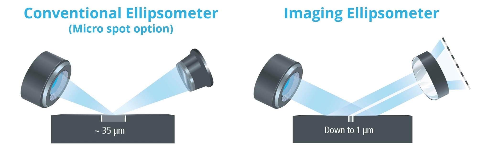
Image Credit: Park Systems
What are the main advantages of Ellipsometry over other metrology tools?
- Non-destructive analysis of multilayer stacks: Ellipsometry can measure complex multilayer systems, whereas other metrology techniques like AFM or WLI mainly capture surface height information and cannot independently resolve buried layers.
- Material-sensitive contrast: Because it is polarization-based, Ellipsometry distinguishes materials based on their optical properties – not just geometry. This allows differentiation of layers with identical topography but different refractive indices.
- Sensitivity to ultra-thin films: Unlike other optical metrology techniques, ellipsometry measures the phase shift induced by very thin layers. This makes it highly sensitive to films at the nanometer and sub-nanometer scales.
Where do conventional, spot-based spectroscopic ellipsometry methods fall short on complex or laterally non-uniform samples?
Conventional, spot-based spectroscopic ellipsometry is extremely powerful for laterally uniform samples, but it runs into clear limitations when samples become complex or spatially varying.
A lack of lateral resolution is one such limit. A single measurement spot averages over the entire beam footprint. On patterned films, thickness gradients, or mixed materials, this averaging can lead to misleading “effective” parameters.
Spot-based ellipsometry also struggles to resolve fine structures. Features smaller than or comparable to the spot size cannot be distinguished, making it impossible to map individual elements.
There is model ambiguity and instability in laterally non-uniform samples, meaning that the measured signal often cannot be described by a single optical model. This reduces fit reliability and may produce non-physical results.
Finally, there are limits in sequential mapping. Spot measurements only provide local information and require multiple sequential measurements to infer spatial trends, which is time-consuming and still risks missing critical defects or gradients.
In short, spot-based ellipsometry struggles whenever spatial averaging hides the true complexity of the sample, making it less suitable for patterned, inhomogeneous, or laterally varying surfaces.
In those scenarios, how does imaging-based spectroscopic ellipsometry (ISE) provide decisive advantages – particularly for spatially resolved thickness and n/k extraction?
In exactly those scenarios, imaging-based spectroscopic ellipsometry (ISE) provides decisive advantages because it adds lateral resolution to the full ellipsometric analysis, rather than relying on spatial averaging:
- Spatially resolved parameter maps: ISE delivers pixel-by-pixel thickness and n/k maps across the field of view. This makes local variations, gradients, edge effects, and defects directly visible rather than averaging them into a single effective value.
- Accurate analysis of patterned and heterogeneous samples: Different materials, pattern elements, or process zones can be evaluated independently within the same measurement. This enables meaningful optical modeling for each region, even on complex layouts.
- Reduced model ambiguity: By separating distinct lateral regions, ISE avoids forcing one global model onto a non-uniform sample. The extracted thickness and optical constants are therefore more stable, physically meaningful, and reproducible.
- High-throughput area coverage: Large areas (e.g., device arrays) can be characterized rapidly and with local detail in a single measurement, eliminating the need for time-consuming spot-by-spot scans.
- Enhanced sensitivity to process-induced variations: Subtle changes in deposition, etching, or functionalization become immediately apparent in spatial maps, enabling tighter process control and faster root-cause analysis. In fact, many users only become aware of local variations after using imaging ellipsometry.
Could you outline a representative ISE workflow on a heterogeneous sample – from field-of-view selection and data acquisition to model fitting and validation?
First, an appropriate field of view is selected to capture relevant patterns, gradients, or material variations.
Next, measurement parameters such as spectral range and angle of incidence are defined, and spectroscopic ellipsometric images are acquired, yielding spatially resolved ellipsometric data for each pixel.
The data are then preprocessed and segmented into regions of interest (ROIs) corresponding to different materials or structures. For each ROI, suitable optical models are defined.
Model fitting is performed pixel-wise or ROI-wise, enabling local extraction of film thickness and n/k of single or multi-layer films, as well as parameter mapping. Finally, the extracted parameters are validated through model consistency checks, residual analysis, and, where necessary, comparison to reference measurements.
How can different regions or inhomogeneities be visualized by ISE even before measurement?
By adjusting the polarization settings, small differences in thickness, material properties, or surface condition are converted into strong intensity contrast, making gradients, patterns, residuals, and defects directly visible across the field of view. This is called ECM (Ellipsometric Contrast-enhanced Microscopy) and is regularly used for ROI identification, visualisation of inhomogeneities, and residual mapping.
One could say that the ISE allows the sample to be viewed with ellipsometric eyes, making it possible to see even sub-nanometer layer thickness differences in the live image.
This provides a quick, model-free overview of sample heterogeneity, enabling reliable selection of regions of interest and planning of measurements before any quantitative analysis is performed. First identify, then measure.
Together with the Stitching tool, it enables mapping of large samples with high sensitivity and high lateral resolution.
Imaging generates dense, spatially resolved spectra. What practices help users quickly and intuitively move from raw images to physically meaningful parameters?
Since spectral data are recorded for each pixel in the field of view, large amounts of data are quickly generated. The most common way to process such large amounts of data is to group pixels with a similar optical response or sample features into regions of interest (ROIs). This reduces noise and enables the application of one optical model per ROI instead of treating every pixel individually.
If regions cannot be clearly identified by the user, our spectral clustering tool can be used. This tool groups pixels with similar spectral ellipsometric responses and can help identify distinct regions or materials before applying an optical model.
For process development and QC, how do you balance lateral resolution, spectral coverage, and acquisition time to make ISE viable day to day?
The key is to optimize the setup for the specific control question rather than always using maximum resolution and full spectral range.
First, the lateral resolution is chosen based on the critical feature size. In QC, pixel binning or moderate magnification is often sufficient, improving signal-to-noise ratio, increasing the measurable area, and reducing data volume while still resolving relevant structures. Full microscopic resolution is reserved for failure analysis.
Second, spectral coverage is tailored to the material system. Instead of measuring the entire available wavelength range, users select the most sensitivity-relevant spectral window. For well-known processes, fixed dispersion models and reduced wavelength sets are often sufficient to extract thickness and key parameters reliably.
Third, acquisition time is optimized through ROI-based analysis and parameter linking. Homogeneous regions can share optical constants while allowing local thickness variation, reducing fitting time. Predefined models and automated workflows further streamline evaluation.
By adapting measurement complexity to the application, ISE becomes a fast, robust, and production-compatible tool rather than a purely research instrument.
Could you share some examples of typical ISE applications?
- 2D Materials: 2D materials (graphene, MoS2, h-BN, etc.) are only one to a few atoms thick and often produced by exfoliation or crystal growth (e.g., CVD), which creates only small flakes in the micron-scale. ISE provides both thickness and refractive index characterization, which is critical for understanding electronic and optical behavior in 2D materials.
- Silicon on Insulator: The ISE provides a full map showing precise local variations on a micron scale across multiple layers. It means that the top silicon layer and the buried oxide layer can be characterized simultaneously with an accuracy of Angstroms using a single measurement. This bridges the gap between spot ellipsometry, which is used for precise multi-layer analysis, and microscopy, which is used for high lateral resolution.
- Biosensors and functionalized surfaces: Many biomolecular layers are only a few nanometers thick. ISE detects subtle changes in thickness and optical constants (n/k), making it ideal for monitoring monolayers, lipid bilayers, or thin polymer coatings. Special accessories enable the detection and measurement of very thin films on transparent substrates, where other optical methods fail due to the back-side reflection of the substrate.
Strategically, what drove Park Systems’ expansion into optical metrology, and how does this broaden the company’s value proposition beyond AFM for advanced materials research?
The move into optical metrology, such as ISE, was not just about adding another tool – it transformed Park Systems from a pure AFM specialist into a comprehensive nanometrology solutions provider, enabling customers to connect surface, optical, and thin-film characterization within an integrated technology ecosystem.
By offering a broader portfolio that includes high-value optical metrology, Park Systems can deepen existing customer relationships, enter new application domains, and compete more directly with larger metrology vendors.
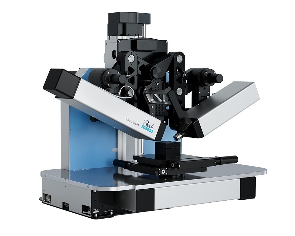
Accurion EP4
Image Credit: Park Systems
About Arash Mirhamed
With more than two decades of dedicated service at Park Systems GmbH (former Accurion GmbH), Arash Mirhamed is a seasoned leader currently heading the ISE Support Team. As a physicist, he transitioned his early expertise in materials science into nearly every stage of the product lifecycle - from the precision of the manufacturing floor to the front lines of applications and customer support.
In his current role, Arash acts as a vital technical catalyst for the company's global expansion. He and his team have played a key role establishing the company’s presence in the field of optical metrology, providing the specialized optical insights necessary for sales and marketing teams to succeed in increasingly competitive international markets.
About Park Systems
Park Systems is a global leader in nanoscale microscopy and metrology solutions, dedicated to empowering scientists, engineers, and industries to push the boundaries of innovation. Built on a pioneering legacy in atomic force microscopy (AFM), the company has grown into the world’s #1 AFM provider and now offers a diversified portfolio that includes imaging spectroscopic ellipsometry (ISE), nanoscale IR spectrometers (AFM-IR), white light interferometry (WLI), active vibration isolation (AVI), and digital holographic microscopy (DHM).
With headquarters in Korea, 16 global offices, and a trusted customer base of leading universities, national labs, and semiconductor fabs, Park Systems is shaping - and expanding - the future of nanometrology.

This information has been sourced, reviewed, and adapted from materials provided by Park Systems.
For more information on this source, please visit Park Systems.
Disclaimer: The views expressed here are those of the interviewee and do not necessarily represent the views of AZoM.com Limited (T/A) AZoNetwork, the owner and operator of this website. This disclaimer forms part of the Terms and Conditions of use of this website.