Sponsored by XradiaApr 22 2013
Xradia's VersaXRM™ 3D X-ray microscope enables high resolution imaging of bump cracks and voids down to submicron levels, even for large packages without any sample preparation.
As the complexity of the package increases, it becomes more difficult to clearly identify failures in sophisticated three-dimensional packages.
Xradia's VersaXRM 3D X-ray microscope offers a unique non-destructive high-resolution capability for imaging buried failure locations. In many cases it can provide enough information to replace or enhance the success rate of physical cross sectioning.
Solder balls or bumps, often made of Pb, Sn/Pb, or recently Pb-free alloys, play the role of interconnecting chips in advanced semiconductor packaging technology such as flip chip, BGA and CSP. Here, the balls replace the traditional pins in connecting the integrated circuit to a circuit board or, in the case of flip chips, bumps connect the chip to the package substrate. Once the chip or package is soldered into place, it becomes very difficult to look for soldering faults since they can no longer be directly observed with optical or SEM inspection without destroying the sample.
Failure Mechanisms
It is possible that a number of failures occur within the bump or at the interface to the substrate or the chip. For example, formation of solder fractures may occur due to thermo-mechanical mismatch between bumps and substrates or gas bubble inclusions may generate solder voids during the reflow process. These two defects are identified as basic failure mechanisms. Stress induced cracks move through interior bumps or along bump and pad interfaces, potentially leading to electrical failure. Voids impact the fatigue life of solder balls and may contribute to crack propagation. These two failure modes become more prevalent in recent finer pitch packages, which tend to have higher current densities and associated higher operating temperatures. Solder joints are also prone to electromigration-induced failures.
The key step for the success of package failure analysis is fault isolation for components that have failed in electrical test is a major step for the success of package failure analysis. For recent advanced package designs, where bumps are smaller and interconnect architectures are more complex, fault isolation and physical analysis have become more challenging. Conventional techniques, such as scanning acoustic microscopy, time domain reflectometry, and thermal imaging, have proven useful in isolating the general vicinity of bump cracks and voids, however, they commonly don't provide spatial information that is accurate enough to precisely guide subsequent physical cross-sectioning. This is sometimes fatal as if the wrong area is cut, there is no second chance. Also, physical cross sectioning can change or contribute to the defect. This causes uncertainty about the true cause of the failure. Along with being destructive, physical cross sectioning provides incomplete 3D information about the defect.
VersaXRM from XRadia
Xradia's VersaXRM line of 3D X-ray microscopes offer a unique non-destructive solution to fill the resolution gap between conventional fault isolation tools and physical cross-section. The VersaXRM enables high-resolution imaging of bump cracks and voids down to submicron levels without any sample preparation. In a number of cases, it is possible to draw a failure conclusion based on 3D X-ray micrographs without the need of destructive, physical cross sectioning. Examples of defects found on a 20 x 20 mm package-on-package (PoP) assembly are presented in Figure 1, where a 2 µm wide bump crack and 2-25 µm voids between the bump-to-circuit board and bump-to-interposer interface are clearly visible.
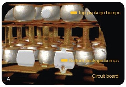
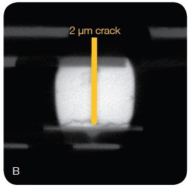
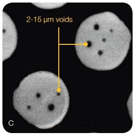
Figure 1. 3D X-ray microscopic images of a package-on-package (PoP) assembly. (A) The 3D micrograph shows the microstructure of the stacked packages; (B) A 2Ijm crack was observed in a bump near the circuit board interface. Courtesy of ST-Ericsson Grenoble Failure Analysis Lab; (C) Multiple voids were found at the interface between the interposer and the top package.
Figure 2 shows the unique advantage of Xradia's systems to maintain high resolution over a large working distance thereby enabling high-resolution topographies, even for larger packages. For other CT systems, the resolution decreases with an increase of sample size, hence an increase in the source-to-center of sample rotation distance. In comparison, the unique architecture of Xradia 3D XRM systems maintains resolution as the working distance increases.
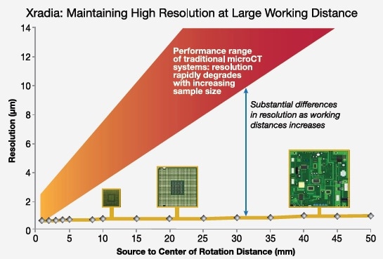
Figure 2. The resolution of conventional MicroCTs decreases as the sample size increases. In contrast, high resolution is maintained at large working distance with Xradia's unique X-Ray microscope architecture.

This information has been sourced, reviewed and adapted from materials provided by Xradia.
For more information on this source, please visit Xradia.