Researchers working at the National Institute of Standards and Technology (NIST) have demonstrated for the first time the existence of a key magnetic-as opposed to electronic-property of specially built semiconductor devices. This discovery raises hopes for even smaller and faster gadgets that could result from magnetic data storage in a semiconductor material, which could then quickly process the data through built-in logic circuits controlled by electric fields.
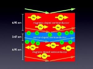 cap Researchers working at NIST have confirmed that thin magnetic layers (red) of a semiconductor separated by a nonmagnetic layer (blue) can exhibit a coveted phenomenon known as "antiferromagnetic coupling," in which manganese (Mn) atoms in successive magnetic layers spontaneously orient their magnetization in opposite directions. This discovery, made by scattering neutrons (arrows) from the material, raises the prospects of "spintronic logic circuits" that could both store and process data. Credit: Brian Kirby, NIST
Magnetic data storage is currently utilized with great success in consumer products such as computer hard drives and MP3 players. But these storage devices are based on metallic materials. These conventional hard drives can only hold data; they have to send the data to a semiconductor-based device to process the data, slowing down performance.
In a new paper,* researchers from NIST, Korea University and the University of Notre Dame have confirmed theorists’ hopes that thin magnetic layers of semiconductor material could exhibit a prized property known as antiferromagnetic coupling-in which one layer spontaneously aligns its magnetic pole in the opposite direction as the next magnetic layer. The discovery of antiferromagnetic coupling in metals was the basis of the 2007 Nobel Prize in Physics, but it is only recently that it has become conceivable for semiconductor materials. Semiconductors with magnetic properties would not only be able to process data, but also store it.
The most widely studied magnetic semiconductor is gallium arsenide (GaAs) with magnetic atoms (manganese) taking the place of some of the gallium atoms. Theorists had predicted that by creating thin films of this material separated by a nonmagnetic material of just the right thickness and electrical properties, one could engineer antiferromagnetic (AF) coupling. With magnetic fields, one could then switch the magnetization of one of the layers back and forth to create “spintronic” logic circuits, ones that operate not only under the usual control of electric fields but also the influence of magnetic fields (manipulating a property known as spin, which could be imagined as tiny internal bar magnets in particles such as electrons).
The team, working at the NIST Center for Neutron Research, studied these multilayer stacks using a technique known as polarized neutron reflectometry. In this technique, a beam of neutrons is bounced off the stacks. Since neutrons are magnetic, and are able to easily penetrate through the entire stack, the reflected neutrons provide information about the magnetic properties of the individual layers. At low temperatures and small magnetic fields, the polarized neutron data unambiguously confirm the existence of an antiparallel magnetic alignment of neighboring layers. When the magnetic field was increased, the neutron data indicated a parallel alignment of all layers. These results demonstrate that AF coupling is achievable in GaMnAs-based multilayers, a seminal property that now opens up a multitude of device possibilities for this novel material. While the phenomenon only occurs at very cold temperatures in the material (about 30 K), the researchers believe these results will help inform theorists who could then better understand how to create room-temperature devices with the same magnetic properties.
* J.-H. Chung, S.J. Chung, S. Lee, B.J. Kirby, J.A. Borchers, Y.J. Cho, X.Liu and J.K. Furdyna, Carrier-mediated antiferromagnetic interlayer exchange coupling in diluted magnetic semiconductor multilayers Ga1-xMnxAs/GaAs:Be. Physical Review Letters, to be published.