Sponsored by QATMAug 4 2017
In the field of scanning electron microscopy (SEM), the electron backscatter diffraction (EBSD) method has developed into a robust tool for the crystallographic analysis of materials. Specifically, the emergence of computer algorithms for the completely automated analysis of diffraction patterns has pushed the method to evolve into a new kind of scanning microscopy technique, known as “orientation imaging microscopy, OIM”1 or “crystal orientation microscopy/mapping, COM”. It applies computer algorithms for the automated analysis of the diffraction patterns.
COM Technique
The COM technique is based on the repeated acquisition of electron diffraction patterns acquired from every point of a scan grid on a flat surface of a steeply inclined sample in the SEM. The automatic analysis of these EBSD patterns yields, for every scan point, the crystallographic orientation and phase and a value representing the quality of the diffraction pattern. Using this data, the microstructure of the scanned area can be recreated.
The resulting crystal orientation maps offer a wealth of information on the sample, including type and distribution of different phases, size, shape and defect condition of grains, type and position of grain boundaries, local crystal orientation and misorientation distribution (texture) and many more. Also, EBSD can be used to examine the structure of crystals, i.e. lattice parameters and lattice symmetry. Using dedicated software, even specifics of the atomic lattice2 and residual stresses3 may be determined.
The EBSD technique permits observation of bulk samples, i.e. no thin foils as in the case of TEM are needed, with an adequately high spatial resolution of around 50 nm. Sample preparation typically is less complicated than TEM and consists of accurate chemical, mechanical or ion-assisted polishing with the aim of creating a plane surface free of any defects. A detailed overview of this state-of-the-art method is given by the book of Schwartz et al.4.
Electron backscatter diffraction patterns which are acquired from bulk samples have many similarities with Kikuchi diffraction patterns acquired from thin foils in the transmission electron microscope (TEM). Figure 1 shows a typical pattern: It contains bright bands (the so-called Kikuchi bands), on a comparatively strong background.
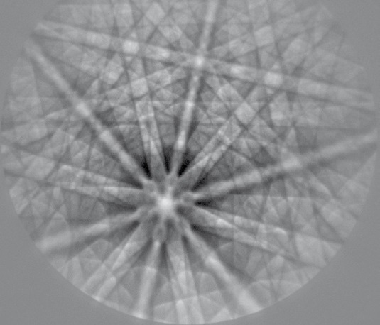
Figure 1. High-resolution EBSD pattern from an as-cast niobium sample (915 x 915 pixel). Exposure time 7 s, with background subtraction.
Each of the bands match a set of lattice planes in the crystal and from the angles between the bands and from their width the Miller indices of these lattice planes can be established. Finally, the crystal orientation and phase can be measured from indexed bands. Patterns are obtained by using a detector which consists of a phosphor screen detected by a highly light-sensitive camera placed in close distance to the sample (20 to 40 mm) as is illustrated in Figure 2.
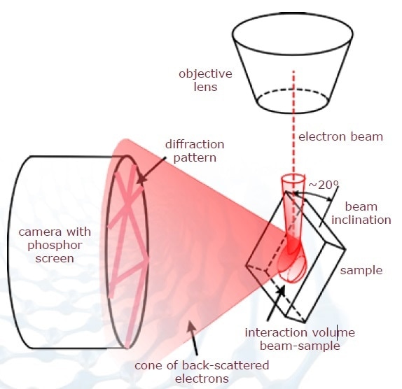
Figure 2. Setup of sample and detector within a scanning electron microscope (SEM).
The detection of band position and the following analysis is performed by fully automated and commercially available software. For COM, the electron beam is moved stepwise over the sample and at every position a pattern is obtained and measured. Measurement and pattern analysis time is usually in the order of 50 to 200 patterns per second. A typical result acquired by COM is illustrated in Figure 3.
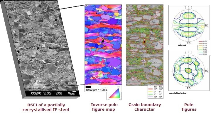
Figure 3. Example of ACOM on a microstructure of a partially recrystallized IF steel. a) Electron channeling contrast image obtained with the backscattered electron (BSE) detector from the untilted sample. b) Diffraction pattern quality map of the observed area. c) Crystal direction map indicating the crystal directions pointing parallel to the sample normal direction (ND). Grain boundaries with misorientation larger than 15° are marked as black lines. d) (111) pole figures of the deformed and recrystallized partition of the sample, showing that recrystallization strongly supports crystal orientations with (111) || ND (center of pole figure). (Courtesy of I. Thomas)
Figure 3 illustrates the microstructure of a partially recrystallized IF steel6 as seen by electron channeling contrast and by COM. In the crystal orientation map similar colors mean similar crystallographic directions pointing towards the sample normal. Grains with uniform orientations (i.e. recrystallized grains) appear in identical colors while grains with internal orientation gradients reveal changing colors.
In this way grain shape and size, recrystallized and non-recrystallized areas, type of grain boundaries and the local texture (in this case shown in the form of pole figures separated for deformed and recrystallized areas) can be easily detected and quantified. The preparation is conducted very gently to obtain a polished surface without deformation. A special mechanism for the generation of the vibrations creates optimum energy transmission to the specimen. Along with the robust design of the SAPHIR 250A1 ECO created by ATM GmbH the vibratory motor ensures noiseless operation.
Since deformation and its associated layers underneath the surface distort the microstructure, a preparation process resulting in a polished surface without artifacts is of great importance. A preparation succeeding a very gentle material removal realizes this ambitious goal. This can be realized using a vibratory polishing device such as SAPHIR 250A1 ECO , illustrated in Figure 4.
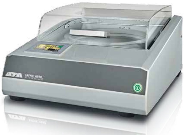
Figure 4. Vibratory polishing device of ATM GmbH: “Saphir 250A1 ECO ”.
Conclusion
Following that kind of approach avoids virtually any kind of deformation by using suitable preparation settings. The material removal is performed by integrating fine grained polishing suspension and polishing cloth together in a vibratory bowl. Thus, the creation of artifacts is prevented and in principle a polished surface without deformation can be analyzed. The results of such an analysis are reliable and reproducible, which is of high significance for studies close to the limits of materialography.
References and Further Reading
- Adams, B.L., Wright, S.I., Kunze, K.: Orientation imaging: the emergence of a new microscopy, Metall. Trans. 24A, 819–831 (1993).
- Wilkinson, A.J., Meaden, G. & Dingley, D. J. (2006): High-resolution elastic strain measurement from electron backscatter diffraction patterns: new levels of sensitivity. Ultramicroscopy, 106, 307–320.
- Winkelmann, A.Trager-Cowan, C.Sweeney, F.Day, A, P. & Parbrook, P. (2007): Many-beam dynamical simulation of electron backscatter diffraction patterns. Ultramicroscopy, 107, 414–421.
- Schwartz, A.J., Kumar, M., Adams, BL. & Field, D. P. (2009): Electron Backscatter Diffraction in Materials Science. Springer, New York
- Zaefferer, S., Habler, G.: Scanning electron microscopy and electron backscatter diffraction, in: Mineral reaction kinetics: microstructures, textures, chemical and isotopic signatures, EMU Notes in Mineralogy, 2016, in print.
- Thomas, I., Zaefferer, S., Friedel, F., Raabe, D.: High resolution EBSD investigation of deformed and partially recrystallized IF steel, Adv. Eng. Mat. 5, 566 – 570 (2003).

This information has been sourced, reviewed and adapted from materials provided by QATM GmbH.
For more information on this source, please visit QATM GmbH.