The research of Prof. Brongersma of the Nanoscale Electronics and Photonics Group at Stanford University is focused on the fabrication and characterization of nanometer-sized electronic and optical devices. In this field, Prof. Brongersma is exploring the optical properties of metallic nanostructures. These structures utilize the distinctive properties of plasmon excitations on metallic surfaces to provide the possibility of transmitting, confining and manipulating light on a scale much smaller than the wavelength of the incident photons.
Metal Nanostructures Possess the Right Combination of Electronic and Optical Properties
For upcoming developments in nanotechnology, it is crucial to provide communication channels that allow controlled information and energy transport at the nanometer level. The design of a dense network of electronic interconnects that can link together huge numbers of nanoscale devices on a chip is not a minor task. Reductions in the pitch and cross-section of metallic interconnects give rise to local heating and an increase in the RC time constant (delay) of interconnected structures.
Optical interconnects do not present such issues. Furthermore, optical interconnects have a much higher information carrying capacity because of their higher operating frequency. Regrettably, conventional optical interconnects do not scale down well. The reduction in size of dielectric optical components is basically limited by the diffraction limit of light. Providing a mechanism that enables optical interconnection with individual nanodevices beyond the limits set by diffraction would immensely expand the information processing capabilities of nanoscale structures.
Metal nanostructures usually possess precisely the right combination of electronic and optical properties to approach these issues to realize the ambition of remarkably faster processing speeds. Cu and Al are the metals commonly used in electrical interconnection; these metals allow the excitation of surface plasmon-polaritons (SPPs). SPPs are electromagnetic waves that propagate along a metal-dielectric interface and are coupled to the free electrons in the metal.
Investigating SPPs Using WITec Scanning Nearfield Optical Microscope
The group of Prof. Brongersma uses the WITec scanning nearfield optical microscope alpha300 S to study these SPPs. The Nanoscale Electronics and Photonics Group at Stanford has modified the alpha300 S into a photon scanning tunneling microscope (PSTM) for experiments on plasmonic waveguides. In the PSTM, SPPs can be excited along a metal structure or interconnect by focusing an excitation laser on the structure using a microscope objective. Using a microfabricated WITec SNOM-cantilever probe, the propagation of the SPPs can be imaged. These probes have a sub-wavelength aperture (about 50 nm diameter) at the apex of a hollow pyramidal tip through which light can be scattered, collected, and then directed toward a photodetector, such as a photomultiplier tube. The detected signal gives a measure of the local light intensity directly underneath the tip, and the propagation of SPPs can be imaged by scanning the tip over the metal surface. The optical resolution attainable with the alpha300 S is in the range of 50–100 nm.
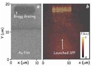
Figure 1. a) SEM image of a Au film into which a Bragg grating has been fabricated using an FIB. (b) PSTM image of an SPP wave launched along the metal film toward the Bragg grating. The back reflection of the SPP from the Bragg grating results in the observation of a standing wave interference pattern.
SPP Wavelengths Determined in a Straightforward Manner Using WITec Alpha300 S
As shown in Figure 1a, the operation of the alpha300 S in PSTM mode can be demonstrated by investigating the propagation of SPPs on a patterned Au film. To define a series of parallel grooves, which serve as a Bragg grating to reflect SPP waves, a focused ion beam (FIB) was used. Shown in Figure 1b is a PSTM image of an SPP wave excited with a 780 nm wavelength laser and directed toward the Bragg grating.
In the image, the back reflection of the SPP from the grating results in the standing wave interference pattern observed. From this type of experiment, the wavelength of SPPs can be determined in a simple way and compared to theory.
To generate 55 nm thick Au stripes on a SiO2 glass slide with stripe widths ranging from 50 nm to 5 µm, electron beam lithography has been used. Au stripes are ideal for fundamental waveguide transport studies because they do not oxidize, are easy to fabricate, and exhibit a qualitatively similar plasmonic response to Al and Cu. Shown in Figure 2a is an optical micrograph of a typical device consisting of a large Au area from which SPPs can be launched onto metal stripes of varying width.
The inset depicts a scanning electron microscopy (SEM) image of a 250 nm wide stripe. The red arrow shows schematically how light is launched from a focused laser spot into a 1 µm wide stripe. PSTM images of SPPs excited at 780 nm and propagating along 3.0 µm, 1.5 µm, and 0.5 µm wide Au stripes are respectively shown in Figures 2b, 2c and 2d. To propagate signals over several tens of microns, the 3.0 µm wide stripe can be used.
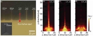
Figure 2. (a) Optical microscopy image of a SiO2 substrate with an array of Au stripes attached to a large launchpad generated by electron beam lithography. The red arrow illustrates the launching of an SPP into a 1 µm wide stripe. (b, c, and d) PSTM images of SPPs excited at 780 nm and propagating along 3.0 µm, 1.5 µm, and 0.5 µm wide Au stripes, respectively.
Imaging SPP Propagation Directly in Plasmonic Structures and Devices Using Alpha300 S
With the alpha300 S used in the PSTM mode, SPP propagation can be directly imaged in plasmonic structures and devices of more complicated architecture to ascertain their behavior. This is relatively different from typical characterization procedures for photonic devices in which the device is seen as a black box with input and output ports. In such cases, the device operation is deduced from responses measured at output ports to various stimuli provided at the input ports. The PSTM provides a clear benefit by providing a direct method to view the inner workings of plasmonic devices, offering a glance inside the box.

This information has been sourced, reviewed and adapted from materials provided by WITec GmbH.
For more information on this source, please visit WITec GmbH.