GFET chips offer scientists direct access to the most recent graphene devices. This supports application-driven research by eliminating the need to develop GFETs from scratch. Each chip includes 36 individual GFETs distributed in distinctive patterns—06-2555: Grid pattern; 06-2560: Quadrant pattern.
Features
- 36 individual GFETs per chip
- Devices not encapsulated ready for customers’ functionalization
- Mobilities typically in excess of 1000 cm2/V.s
- Ideal platform device for the research and development of new sensors
Applications
- Graphene device research
- Bioelectronics
- Chemical sensors
- Magnetic sensors
- Biosensors
- Photodetectors
Typical Specifications
| . |
. |
| Chip dimensions |
10 mm x 10 mm |
| Chip thickness |
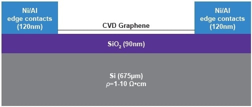
675 μm |
| Number of GFETs per chip |
36 |
| Gate Oxide thickness |
90 nm |
| Gate Oxide material |
SiO2 |
| Resistivity of substrate |
1-10 Ω.cm |
| Metallization |
Nickel/Aluminium 140 nm |
| Graphene field-effect mobility |
>1000 cm2/V.s |
| Residual charge carrier density |
<2 x 1012 cm-2 |
| Dirac point |
10-40 V |
| Yield |
>75 % |
Device Cross-Section
Typical Characteristics
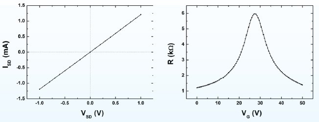
Output curve (left) and transfer curve measured at source-drain voltage of 20 mV (right), measured at room temperature and vacuum conditions on a device with W = L = 50 μm.
Absolute Maximum Ratings
| . |
. |
| Maximum gate-source voltage |
± 50 V |
| Maximum temperature rating |
150 °C |
| Maximum drain-source current density |
107 A.cm-2 |
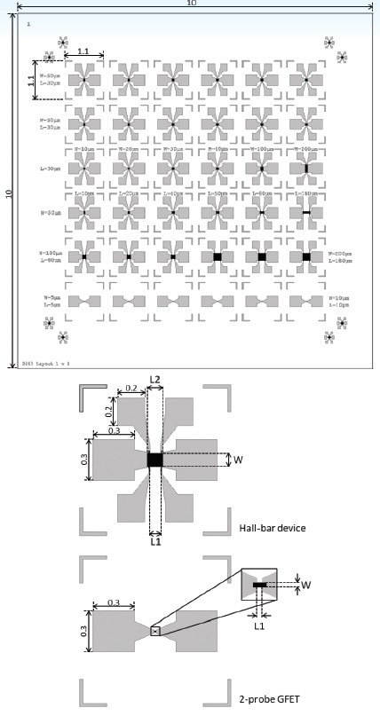
06-2555: GFET chip—grid pattern
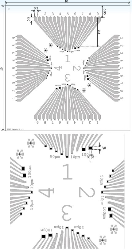
06-2560: GFET chip—quadrant pattern
Channel Geometries
| Description |
W (μm) |
L1 (μm) |
L2 (μm) |
Quantity |
| Standard |
50 |
30 |
50 |
12 |
| Varying Width |
10 |
30 |
50 |
1 |
| 20 |
1 |
| 30 |
1 |
| 40 |
1 |
| 100 |
1 |
| 200 |
1 |
| Large Square |
100 |
80 |
100 |
3 |
| 200 |
180 |
200 |
3 |
| Varying length |
50 |
10 |
30 |
1 |
| 20 |
40 |
1 |
| 40 |
60 |
1 |
| 50 |
70 |
1 |
| 80 |
100 |
1 |
| 180 |
200 |
1 |
| Small 2-probe |
5 |
5 |
-- |
3 |
| 10 |
10 |
-- |
3 |
| Device number |
W (μm) |
L (μm) |
| 1 |
50 |
50 |
| 2 |
| 3 |
| 4 |
| 5 |
| 6 |
10 |
10 |
| 7 |
| 8 |
100 |
100 |
| 9 |

This information has been sourced, reviewed and adapted from materials provided by Strem Chemicals.
For more information on this source, please visit Strem Chemicals.