The manufacture of semiconductors continues to advance quickly, as predicted by Moore’s Law, with each new generation of technology decreasing the spacing and size of layers and features on the integrated circuits (ICs).
Image Credit: Superior Sensor Technology
This higher density of circuitry on a wafer requires greater accuracy and a highly fragile and advanced fabrication process.
Several newer and highly complex ICs today are made of a dozen or more layers produced in 300+ sequenced processing steps. As soon as the wafers have been fabricated, the next step is post-processing, followed by IC packaging and testing.
Given below is a summary of a few of the traditional steps in the IC manufacturing process:
- Wafer processing
- Surface passivation
- Photolithography
- Cleaning of the silicon wafers
- Various depositions (atomic, chemical, physical)
- Wafer testing
- Etching
- Die preparation
- Wafer mounting
- Wafer back grinding and polishing
- Wafer bonding and stacking
- Die-cutting
- Wafer bumping (if required for flip chips)
- Through-silicon through (TSV) manufacture (if needed for 3D ICs)
- IC packaging
- Die attachment to a substrate
- IC bonding (like wire bonding)
- Comes with laser marking and silkscreen printing
- IC encapsulation
- IC Testing
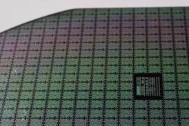
Figure 1. Image of Silicon Wafer with Etched Circuitry. Image Credit: Superior Sensor Technology
Nowadays, the manufacturing of semiconductors places remarkably high demands on pressure measurement technology to ensure a high-quality process. All fabrication steps, such as cleaning, etching and polishing, should be as precise as possible as the finished product uniformity is quantified in microns.
At the same time, testing and inspection are performed to quantify variances during all phases of semiconductor manufacturing.
The Role of Pressure Sensors in Semiconductor Manufacturing
Pressure sensors are used across IC manufacturing to perform real-time pressure measurement across the various stages of the semiconductor process. A few of the general uses include:
- Improving the accuracy and control of the wafer polishing heads by constantly applying pressure. As far as chemical mechanical polishing (CMP) systems are concerned, measurements like parallelism of the polishing heads and characterization are considered a crucial part of the fabrication process.
- Guarantee persistent wafer cleaning by checking how effective the wafer polishing head is. If the polishing head is not conditioned correctly, or it is lacking an even roughness on its surface, the elimination of external particles will not be efficient. Any particle residue might lead to ICs fail inspection and test.
- Restricting the amount of cracked or unbounded wafers. As stated, CMP is considered a key manufacturing process for semiconductors, as improving uniformity throughout the polishing process is crucial. A polishing head that is uneven can lead to cracks appearing in the wafer, resulting in ICs being rejected.
- Confirm die-to-substrate planarization, especially for flip-chip bonding. Even pressure is required to avoid die cracking or open electrical connections. As with wafer cracking, an IC with a damaged die or open electrical connection cannot be utilized.
- Discerning wear on plates and other parts can result in wafer bonding errors. To employ level amounts of pressure via the attachment process, the plates should be even. But like other components, they do wear over time which may lead to non-uniformity. By identifying the pressure variations, the equipment can identify the issue and sound a repair alarm before faulty parts are assembled.
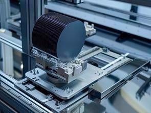
Figure 2. Image of Wafers in Fabrication. Image Credit: Superior Sensor Technology
Superior Sensor’s NimbleSenseTM Architecture for Semiconductor Manufacturing
With an extremely low noise floor, the NimbleSense architecture is perfect for the accurate pressure measurements demanded by semiconductor equipment to improve long-term stability, optimize precision and increase overall IC production yields.
But, the advantages of NimbleSense extend well beyond the low noise floor. A few of its application-specific building blocks provide additional value add for semiconductor manufacturing.
Multi-Range TechnologyTM
Multi-Range technology enables just one pressure sensor to work over several pressure ranges. As wafer lots possess numerous layers, and bonding or packaging can differ, the pressure requirements tend to vary.
Multi-Range enables one sensor to be adjusted without any degradation in performance to fulfill the pressure demands for various fabrication processes.
Advanced Digital Filtering
Semiconductor manufacturing demands accuracy, and external factors, such as noise from air conditioning or other equipment, building vibrations, etc., can severely impact the precision of pressure sensors.
Making use of Superior’s integrated advanced digital filtering technology, these pressure sensors remove noise before it reaches the fabrication process. Therefore, the noise is eliminated before it becomes an error signal that can produce inaccurate readings.
Conclusion
Semiconductor manufacturing is progressing at a rapid pace, with each new generation of technology decreasing the size and spacing of features and layers on ICs.
This increased density of circuitry on a wafer puts extremely high demands on pressure measurement technology to ensure a high-quality process. Every step involved in the fabrication process should be performed to the highest degree of accuracy as the uniformity of the completed product is quantified in microns.
Superior Sensor’s specialized pressure sensor technology, based on proprietary NimbleSense architecture, provides various advantages for semiconductor equipment, such as remarkable long-term stability, greater precision, advanced digital filtering and Multi-Range technology.
To discover more about the NimbleSense architecture, users can visit Superior’s technology page, or contact Superior Sensor to discuss a semiconductor-related project.

This information has been sourced, reviewed and adapted from materials provided by Superior Sensor Technology.
For more information on this source, please visit Superior Sensor Technology.