FilmTek 2000 PAR-SE combines proprietary FilmTek™ technologies to independently measure film thickness and refractive index with exceptional resolution. Using specialized, non-contact optical methods, the system collects multi-angle, multi-modal data and applies patented modeling and data processing to deliver results in seconds - supporting real-time process control.
Designed for automated, inline measurement, the FilmTek 2000 PAR-SE is optimized for patterned thin films and complex multilayer stacks. It’s well-suited for advanced device structures, including ONO stacks, high-k and low-k materials, polycrystalline and amorphous silicon, and SiGe.
The system is equipped with advanced material modeling software, offering a fully integrated solution that simplifies even the most demanding measurement tasks - whether on blanket or patterned wafers.
The FilmTek 2000 PAR-SE delivers a combination of:
- Unmatched measurement precision with sub-angstrom thickness repeatability and high-resolution refractive index analysis - even at high spatial resolutions
- Versatile application capabilities for automated inline measurement of ultrathin films in complex multilayer stacks, including those traditionally considered difficult to characterize
- Advanced material modeling that goes beyond basic thickness and refractive index, providing deeper insights into properties like surface roughness, crystallinity, and bandgap
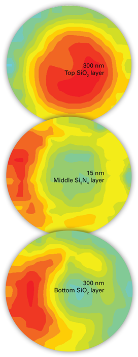
Image Credit: Bruker Nano Surfaces and Metrology
Multi-Modal Optical Thin-Film Metrology
Bruker’s FilmTek tools tackle applications that go beyond the capabilities of traditional ellipsometry and reflectometry. The FilmTek 2000 PAR-SE uses a multi-angle, multi-modal approach to deliver independent and unambiguous measurements of both the refractive index (n) and extinction coefficient (k). It also provides precise, repeatable film thickness measurements - ranging from angstrom-level native oxides to thick films up to 150 µm, and from single layers to complex multilayer stacks.
The FilmTek 2000 PAR-SE features a rotating-compensator ellipsometer, patented parabolic mirror technology, and deep UV (DUV) multi-angle reflectometry - hardware that powers Bruker’s patented technologies for advanced thin-film metrology.
- Multi-Angle Differential Polarimetry (MADP): Integrates reflectometry (0°) and ellipsometry (70°) at the same location, allowing precise and independent determination of thickness and refractive index, even for ultra-thin films.
- Multi-Angle Differential Power Spectral Density (DPSD): Uses polarized reflectometry spectra at both normal (0°) and oblique (70°) incidence to measure thickness and index, providing the best index resolution compared to other methods
The combination of these unique hardware components and core technologies delivers impressive performance, including thickness repeatability of 0.03 Å for thin films, highly accurate reflection measurements across a wide wavelength range, and high spatial resolution for precise targeting.
Multi-modal reflectance and ellipsometry data of 900 nm SiC on 1800 nm SiO2 on Si substrate. Image Credit: Bruker Nano Surfaces and Metrology
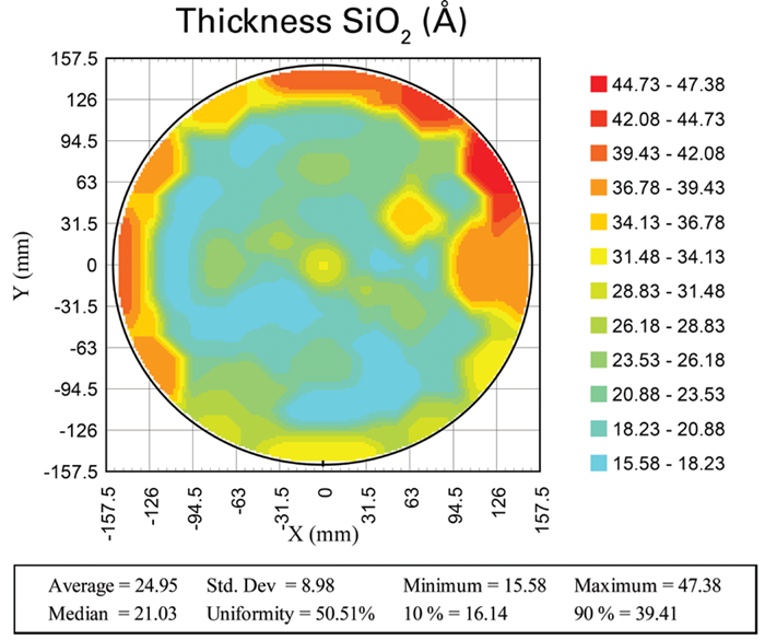
Uniformity mapping of ultrathin SiO2 on Si substrate. Image Credit: Bruker Nano Surfaces and Metrology
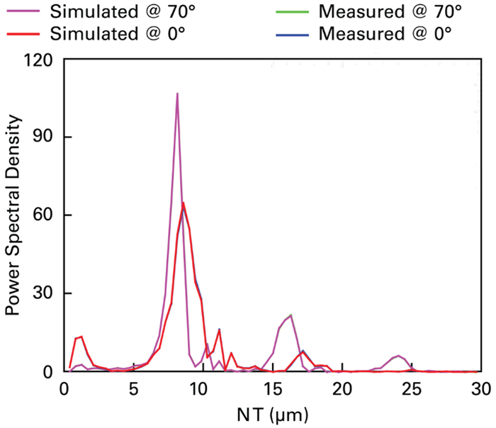
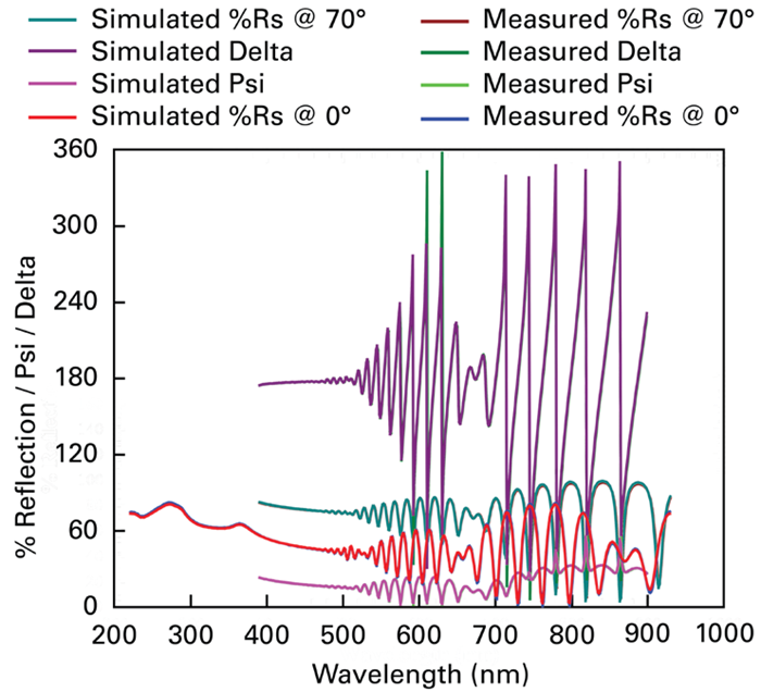
DPSD plot of 900 nm SiC on 1800 nm SiO2 on Si substrate to gain accuracy in thickness determination. Image Credit: Bruker Nano Surfaces and Metrology
Advanced Fitting to Resolve Multilayer Thickness and Improve Thickness Accuracy
Traditional ellipsometry determines refractive index by measuring changes in polarization, a process that can be time-consuming and often yields multiple possible solutions. Bruker’s FilmTek tools take a more efficient and direct approach, using wavelength shift and amplitude changes as a function of angle to produce a single, precise, and repeatable result in seconds.
The system also incorporates the DPSD technique, which transforms standard reflectance spectra into a power spectral density plot. This not only improves refractive index determination, but also adds a robust fitting method for accurately measuring single-layer and multilayer film thicknesses.
Fully Automated High-Throughput Small-Spot-Size Inline Metrology
The FilmTek 2000 PAR-SE features a patented parabolic mirror optical design, automated alignment for both 0° and 70° measurement beams, and Cognex PatMax pattern recognition. Together, these enable the high stage accuracy and beam alignment needed to measure within small metrology pads.
An optional configuration is available to reduce the spot size to 25 × 25 μm2, meeting advanced roadmap requirements.
With patented data processing and modeling, the system delivers results within seconds, providing real-time feedback on key parameters for process control.
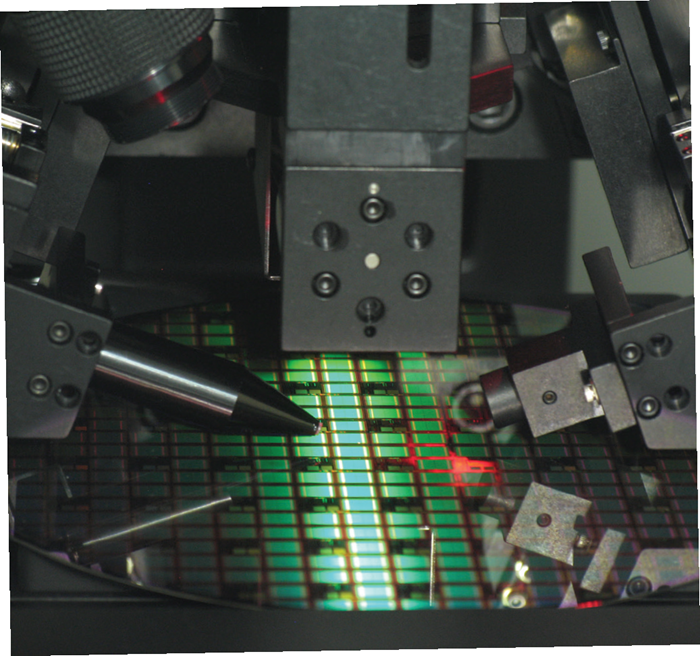
Image Credit: Bruker Nano Surfaces and Metrology
Source: Bruker Nano Surfaces and Metrology
| FilmTek 2000 PAR-SE Robotic Specifications |
| Measurement Function |
Film thickness, index of refraction (n) and extinction coefficient (k), roughness, crystallinity, composition (e.g., %Ge in SiGe) |
| Material Capability |
Al2O3, AlGaAs, AlGaN, AlN, amorphous Si, GST, InGaAs, ITO, IZO, La2O3, LiNbO3, LiTaO3, Mo, MoOx, Nb2O5, photoresist, polyimide, poly-Si, SiO2, Si3N4, SiC, Ta2O5, TiO2, WOx, ZnO, ZnO, ZrO2, and more |
| Film Thickness Range |
0 Å (bare substrate) to 150 μm |
| Film Thickness Accuracy |
±1.0 Å for NIST traceable standard oxide 100 Å to 1 μm |
| Film Thickness Precision (1 σ) |
0 to 1000 Å Oxide/Si (t): 0.03 Å |
| Spectral Range |
220 nm to 1000 nm (optional 190 nm to 1700 nm) |
| Spectral Resolution |
Visible: 0.3 nm; NIR: 2 nm |
| Measurement Spot Size |
50 μm (optional 25 μm) |
| Light Source |
Regulated deuterium-halogen lamp (2000 h lifetime); Lamp change <15 minutes |
| Detector |
2048 pixel Sony linear CCD array; Optional 512 pixel cooled Hamamatsu InGaAs CCD array (NIR) |
| Automated Stage |
200 mm standard or 300 mm optional |
| Measurement Time |
<2 seconds per site (e.g., oxide film) |