Originally introduced in 1974 [1], Deep Level Transient Spectroscopy (DLTS) remains the most sensitive method for characterizing deep level traps caused by impurities and electrically active defects in both traditional and more exotic semiconductor materials, structures and devices. Characterizing these traps allows a researcher to begin to control and tune the impact of these impurities and defects. Semilab has been offering leading edge DLTS equipment since the company’s founding in 1989.
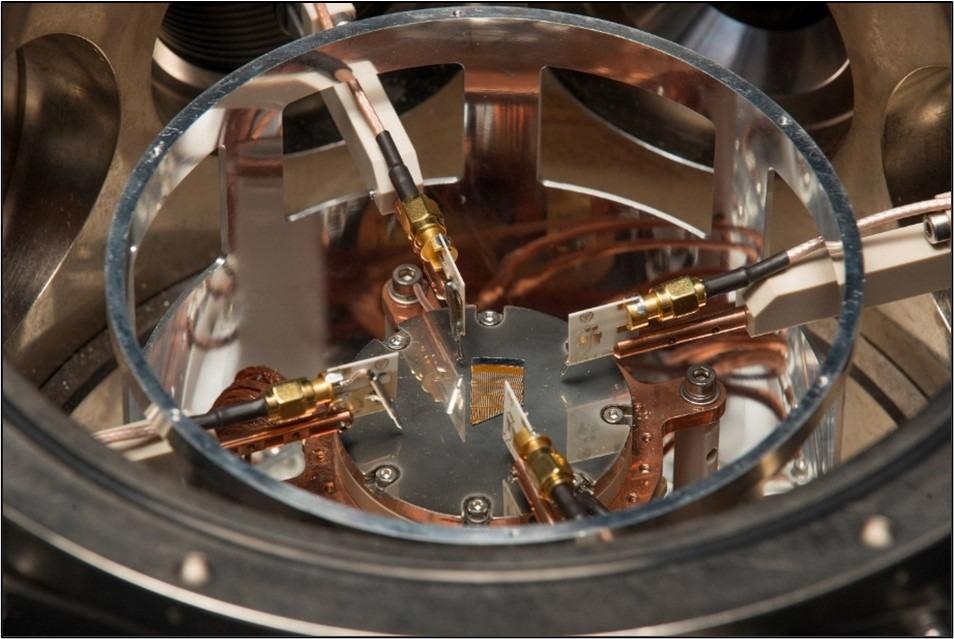
A DLTS measurement consists continuous capacitance measurement after voltage or current pulses taken at different temperatures. A deep level trap is identified as a change in the capacitance signal at a particular temperature. The temperature at which the trap is seen is related to the characteristic activation energy of the trap. Several different cryostats ranging from a simple LN2 bath (~77K) to a low vibration closed cycle He cryostat (30K -> 800K) are available to allow measurements on a wide variety of semiconductor materials.
DLTS is widely used for contamination analysis in silicon epitaxial layers, particularly for:
- Raw Si material (wafer fragment)
- Bi-CMOS/DMOS devices
- CMOS image sensor (CIS)
- Charge-coupled device imagers (CCD)
The technique has also been used for non-silicon materials:
- Silicon Carbide – power semiconductor, betavoltaic devices
- Gallium Arsenide - RF
- Germanium
- Gallium Nitride
- Piezoelectrically formed 2D Electron Gas (2DEG)
- Materials used for InfraRed sensors and focal place arrays (InGaAs, GaSb, HgCdTe).
DLS-1100 & DLS-83D
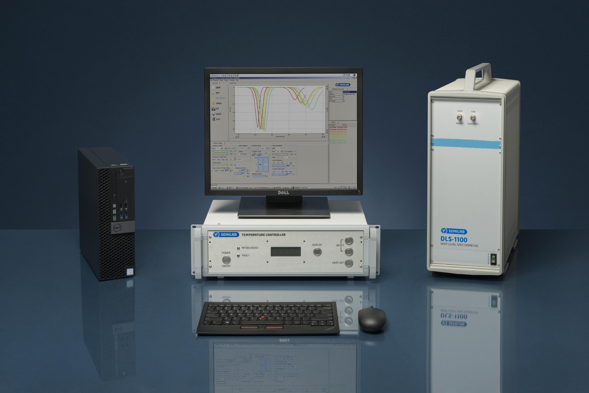
Semilab offers two DLTS measurement systems, the DLS-83D and the DLS-1100 systems. Both systems provide a turnkey automatic DLTS measurement with software to assist in the interpretation and identification of the measure curves, allowing researchers to focus on engineering their materials. The Windows 10 based WinDLS software automatically identifies and measures many traps with an extensive material library. Several modes, including transient digitization are available to facilitate the differentiation and characterization of different trap states.
The DLS-83D is the ideal choice for academic research as it provides good sensitivity at a low price. The DLS-1100 has a lower noise floor, and is the leading high-sensitivity measurement system for silicon wafer manufacturers and the most advanced R&D purposes.
Full Range of Measurement Modes
- Temperature scan
- Frequency scan
- Direct transient recording & digitization
- Current-DLTS (I-DLTS)
- Optical excitation (Optical-DLTS)
- Depth profiling
- I-V, C-V & G-V characterization
- Activation energy & Capture cross-section measurement
Windows 10 based WinDLS software allows fully automated data acquisition and temperature control during operation
- Wide-ranging software support including customized automation of measurement sequences,
- Full library database for accurate contamination identification
Features and System Specifications
- Maximum sensitivity (2×10⁸ atoms/cm3) for detection of trace levels of contamination
- Wide range of cryostats selection with different temperature ranges:
- Low vibration cryostat chamber <30K-400K (optionally up to 800K)
- Closed Cycle He-cryostat from <30K to 325K
- Automatic LN2 cryostat with controlled LN2 flow from 80K to 800K
- Bath type LN2 cryostat 80K-450K
- Controlled by analog and digital settings to allow operational ease
- Complete computer control with wide-ranging software support, full library database for accurate contamination identification
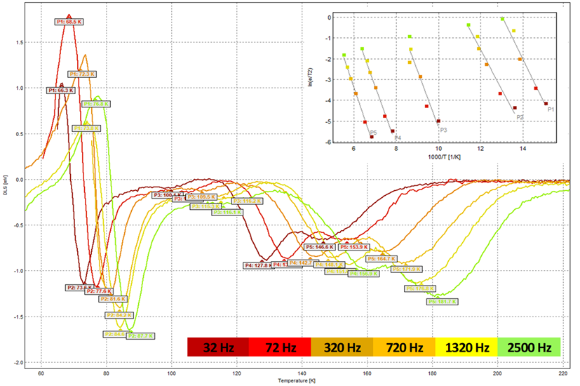
Measurements on Mg2Si - Temperature-scans and corresponding Arrhenius-plots at various Lock-in frequencies. Image credit: Semilab
The DLS-1100 system is the market leading DLTS solution for industrial semiconductor production. Thanks to the outstanding signal to noise ratio of the main measurement unit, uniquely high sensitivity can be achieved in impurity detection (below 2*108 atoms/cm3). The DLS-1100 provides a fully automatic measurement mode and complete interpretation of the measured data, including concentration determination and impurity identification with minimal need for user interaction.
The DLS-1100 is a versatile system for monitoring and characterizing deep levels caused by defects and impurities in complete devices and semiconductor materials. This system is suitable for determining all parameters related to deep traps including capture cross section, energy level, and concentration distribution. SEMILAB DLS systems support transient digitization, therefore improves and facilitates differentiation and characterization of trap states.
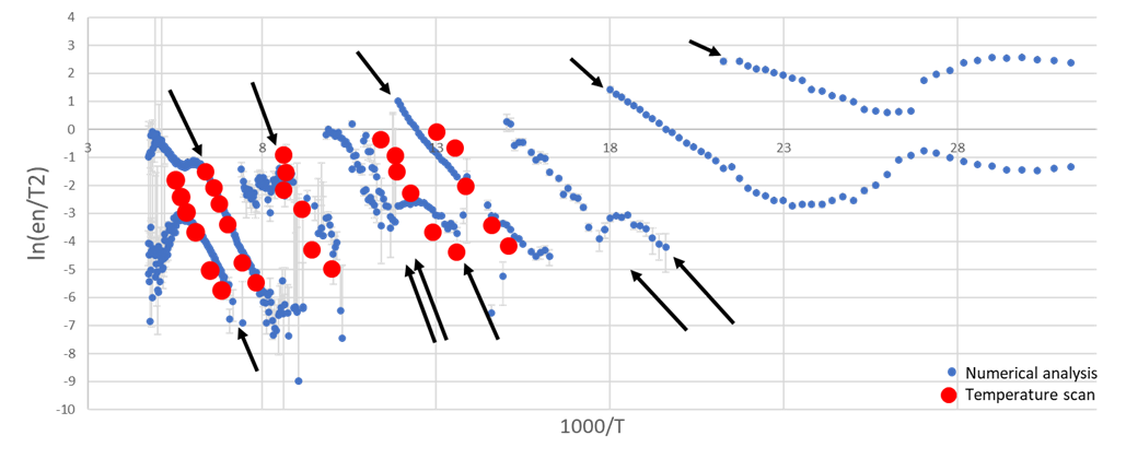
Measurements on Mg2Si - Arrhenius plot based on digital numerical analysis & temperature-scan analysis. Possible trap levels revealed by digital transient analysis are marked by arrows. Image credit: Semilab
References:
[1] D. V. Lang, “Deep‐level transient spectroscopy: A new method to characterize traps in semiconductors,” J. Appl. Phys., vol. 45, no. 7, pp. 3023–3032, Jul. 1974, doi: 10.1063/1.1663719