Semilab offers a unique modular optical platform, the SE-2000, which includes a spectroscopic ellipsometer with rotating compensator optics. It performs non-destructive and non-contact optical measurements on substrates, single layer and multi-layer samples to obtain individual thin film thickness and optical properties.
Key Features
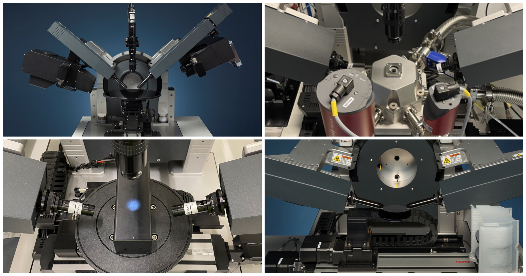
The key features of the SE-2000 are:
- The system has a robust, versatile and modular design and enables studying samples from simple single layer thickness to more challenging applications such as those combining polarimetry, scatterometry and ellipsometry using Mueller matrix.
- It has an innovative independent arm angle selection and a small spot size.
- The SE-2000 offers a wide spectral range ranging from the Deep-UV (193nm) up to Mid-IR (25µm) with optional FTIR ellipsometer head uniquely offered on the same goniometer with the visible arms.
- It can either be configured with the fast detection mode using spectrograph and detector array, or with the high resolution one using spectrometer and single point detectors, or with both modes combined together in a single tool.
- SE-2000 includes Semilab’s new smart electronics with interchangeable components, and operates with the new generation operating and analysis software (SAM/SEA).
- The system can be controlled from a PC or Laptop through LAN Network, or by a new touch panel interface.
Measurement Modes
Measurement modes include the following:
- Spectroscopic Ellipsometry for thin film thickness and optical functions, including complex multilayer structures
- Generalized Ellipsometry for Anisotropic materials
- Transmission Ellipsometry for transparent substrates
- Scatterometry vs. wavelength and angle of incidence
- Mueller Matrix (11 or 16 elements) uniquely offered in combination with Scatterometry for 3D anisotropic materials
- Jones Matrix for simple anisotropic materials
- Reflectance and Transmittance vs. wavelength and incidence angle
- Polarimetry
- Porosimetry: Measurements of pore size and porosity in thin films
- In-situ measurement mode for real time control during deposition or etch process
Applications
The SEMILAB SE-2000 provides measurement to the following application fields:
- Photonics - LED, optronics: AlGaN, GaN, InP, etc,Reflective Coatings, ARC, III-V devices (EEL, VCSEL, ECL),MEMS andSol-Gel/Porous coatings
- Photovoltaics -Thin films and Silicon solar cell, Nanostructured Cells, transparent conductive oxide, nanodots, nanowire, CNT
- Organics - OLED, OPV, sensors, OTFT
- Semiconductors - High-k, Gate Oxide, Nitride oxide,Low-k, Interconnects, Lithography thins films, Epi-layers: SOI, SiGe, Strained Si, SiC, Poly
- Flat Panel Displays - TFT-LCD, LTPS, IGZO, OLED, electrochromic layers
- General - Ferroelectric materials (BST, SBT, PZT), Fuel cells, SOFC, porous electrode, graphene, 3D materials, periodic structures