The PlasmaPro 100 Cobra ICP RIE system uses a high-density that has been inductively coupled plasma for quick etch rates to be obtained. The process modules provide high-throughput, outstanding uniformity, high-precision, and low-damage processes for wafer sizes ranging up to 200 mm. This helps in several markets, such as GaAs and InP laser optoelectronics, SiC and GaN power electronics/RF, and MEMS and sensors.
The PlasmaPro 100 Cobra ICP RIE system includes:
- High etch rate and high selectivity is provided
- Low damage etch and high repeatability processing could be performed
- Consistent with all wafer sizes ranging up to 200 mm
- Extensive temperature range electrode, –150 °C to 400 °C
- He backside cooling for improved temperature control
- Rapid change between wafer sizes
- Availability of a single wafer load lock or clusterable with up to five process modules
- In-situ chamber cleaning and end-pointing

Image Credit: Oxford Instruments Plasma Technology
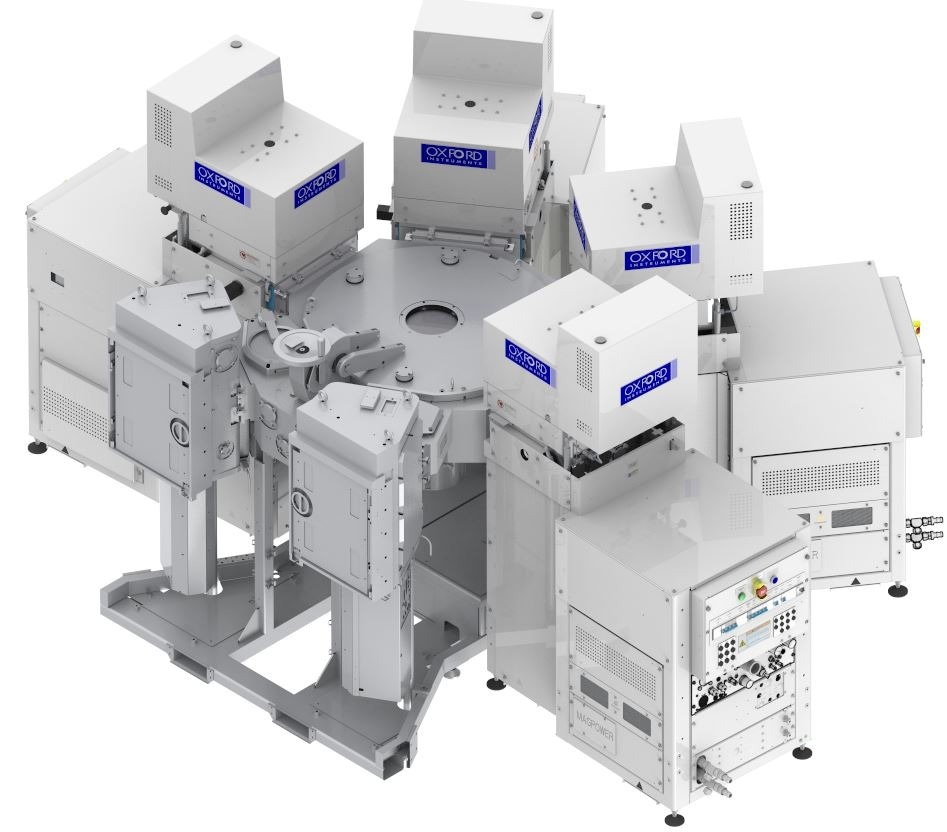
Image Credit: Oxford Instruments Plasma Technology
Overview
The Cobra® ICP plasma source generates high-density reactive species at low pressure. Substrate DC bias is determined by a separate RF generator, enabling independent control of radicals and ions, as per the process needs.
The PlasmaPro 100 process modules from Oxford Instruments provide a 200 mm platform with multi-wafer batch capability and a single wafer. The process modules provide high precision, high throughput, and outstanding uniformity with clean smooth vertical profiles and etch surfaces. The systems have an extensive install base inside high volume manufacturing (HVM), with well-developed process solutions.
Features
- Offers reactive species to the substrate, with an even high conductance path via the chamber—Enables a high gas flow to be utilized while retaining low chamber pressure, offering an extensive process window for progressed application development.
- Wide temperature range electrode that could either be cooled by a fluid re-circulating chiller to −20 °C and liquid nitrogen to −150 °C, or resistively heated to 400 °C—An optional blowout and fluid exchange unit can automate the process of switching modes and −20 °C to −150 °C transition can take just 10 minutes.
- Wafer clamping with He backside cooling—Improved wafer temperature control
- ICP source sizes of 65 mm or 300 mm—300 mm source provide excellent process uniformity up to 200 mm wafers.
- A fluid-controlled electrode fed by a re-circulating chiller unit—Outstanding substrate temperature control
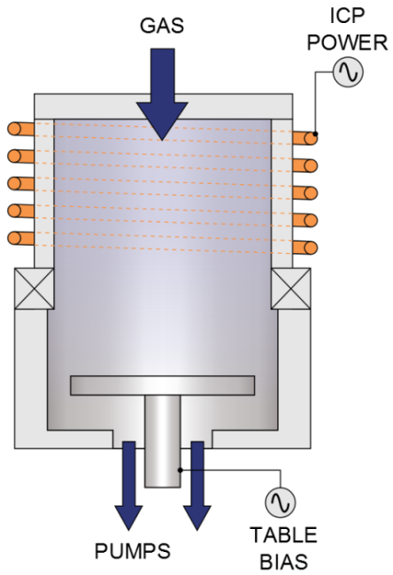
Image Credit: Oxford Instruments Plasma Technology
Applications
- NbN and Ta available for Quantum devices
- Wide library of III-V etch processes
- Compound Semiconductor Applications:
- VCSEL GaAs/AlGaAs etch
- Power electronic/RF SiC, and GaN etch
- Solid State Lasers InP etch
- Extensive library of metal etch process: Cr, Al, Ni, etc
- Si etch
- SiOx and SiO2 etch
- SiO2 and SiNx hard mask etch
- Fused silica and quartz etch available
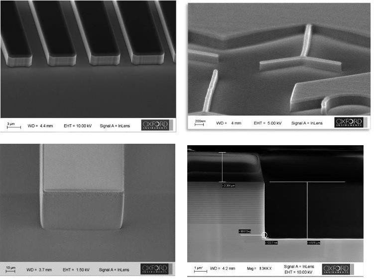
Image Credit: Oxford Instruments Plasma Technology
Specifications
- Wafer size: ranges up to 200 mm
- Temperature range: ranges from −150 up to 400 °C
- ICP source sizes available: 65 mm and 300 mm
- Cluster with: up to five modules, such as PECVD, ALD, Ion Beam Etch, and Ion Beam Deposition technologies.
Options
Other PlasmaPro 100 Systems include:
PlasmaPro 100 RIE
- The RIE modules provide anisotropic dry etching for a wide range of processes.
PlasmaPro 100 ICPCVD
- The ICP CVD process module has been developed to produce high-quality films from room temperature to 400 °C with high-density plasmas at low deposition temperatures and pressures.
PlasmaPro 100 PECVD
- The PECVD process modules are mainly developed to produce outstanding uniformity and high-rate films, with control of film properties, such as electrical characteristics, refractive index, stress, and wet chemical etch rate.