Atomfab from Oxford Instruments offers quick, low damage, low CoO production plasma ALD processing for GaN power and RF devices.
ATOMFAB ALD System - Oxford Instruments Plasma Technology
Video Credit: Oxford Instruments Plasma Technology
PACE
Atomfab is known to be the quickest remote plasma production ALD system that is commercially available.
Solutions for Production Needs
- Competitive CoO
- Outstanding film uniformity
- High material quality
- Fast, easy maintenance
- Quicker cycles times, high throughput
- Clusterable and automated wafer handling
- Low substrate damage
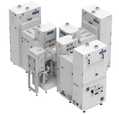
Image Credit: Oxford Instruments Plasma Technology
Performance
Atomfab's ALD technology provides accurately controlled ultra‑thin films for sophisticated applications on the nanometer scale, with a conformal coating of sensitive substrate structures.
Process Benefits for Passivation of Power and Rf Devices
- Plasma surface pre-treatments
- High quality deposition with low film contamination
- Low particle levels
- Guaranteed processes setup by our engineers
- Lifetime process support for additional/new processes
- Low-damage plasma processing
- Short plasma exposure times that allow for high throughput
Advantages of Plasma ALD for GaN, Power, and RF Devices
- Remote plasma ALD with controlled ion energy from near zero to 30 eV
- With plasma pre-treatment prior to deposition to enhance interface quality
- Low damage, uniform deposition
- ALD passivation, gate dielectric by Al2O3 films
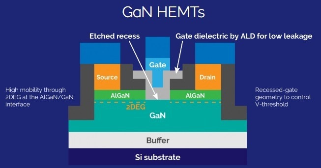
Increased throughput and improved uniformity to bring remote plasma ALD to production. Image Credit: Oxford Instruments Plasma Technology
Plasma
Revolutionary plasma source: Atomfab makes use of a patent-pending remote source that has been specifically developed for atomic-scale processing.
- Low damage for sensitive substrates for utmost device performance
- Short plasma times (250 milliseconds) enabled by patent-pending AMU
- Low reflected power and reproducible strike time for high yield
- Short strike time (80 milliseconds) for high throughput
- Quick cycle times and reliability with even film deposition and plasma exposure
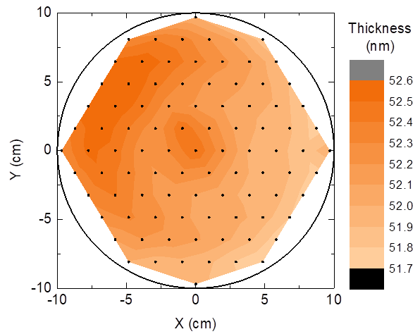
| Plasma ALD Al2O3 at 300 °C |
Specification |
| Within wafer thickness uniformity |
<± 1.0% |
| Wafer-to-wafer thickness repeatability |
<± 1.0% |
| Breakdown voltage |
≥ 7.0 MV/cm |
Image Credit: Oxford Instruments Plasma Technology