The PlasmaPro 100 RIE modules from Oxford Instruments help deliver isotropic and anisotropic dry etching for a wide range of processes. These modules are ideal for research and production customers, providing a controlled environment that enhances process repeatability with load-lock and cassette-to-cassette options.
- Compatible with all wafer sizes ranging up to 200 mm
- Quick change between wafer sizes
- Outstanding uniformity, high throughput, and high accuracy processes
- Wide temperature range electrode, from −150 °C to 400 °C
- In-situ chamber cleaning and end-pointing
- Single-wafer or batch processing available with outstanding process control
- High control of the gases and plasma power
- Simple serviceability and low cost of ownership
Overview
Reactive Ion Etch (RIE) is a physical etch process. A rich plasma has been made just above the wafer, and the ions are expedited toward the surface to generate a highly powerful anisotropic etch.
Using a wafer-level RF source, gas penetrates the top of the chamber, where it is transformed into a reactive plasma at low pressure. The ions either interact with the sample to develop etch by-products or stay as unreacted species. All the unreacted species and by-products are removed from the chamber by the vacuum pump to maintain a rich and active plasma to maintain high etch rates.
The PlasmaPro 100 RIE gives reactive species to the substrate, having an even high conductance path via the chamber, thereby enabling a high gas flow to be utilized while low pressure is retained.
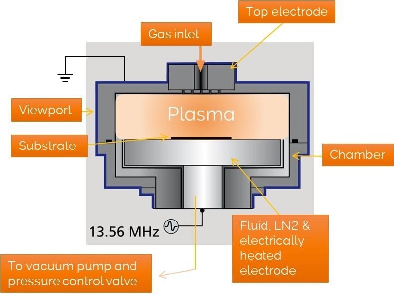
Image Credit: Oxford Instruments Plasma Technology
Features
- Wide temperature range electrode (-150°C to +400°C) that can be cooled using liquid nitrogen, a fluid re-circulating chiller or resistively heated. An optional blow out and fluid exchange unit can automate the process of switching modes
- A high pumping capacity gives a wide process pressure window
- A fluid-controlled electrode that is powered by a recirculating chiller unit and provides excellent substrate temperature control
- Single or double cassettes available with a variety of handler options
- Reactive species to the substrate with a uniform high conductance path through the chamber
- Wafer clamping with He backside cooling for optimum wafer temperature control
- Option of a highly reliable vacuum transfer robot
Applications
- Solid State Lasers InP etch
- III-V etch processes
- VCSEL GaAs/AlGaAs etch
- RF device low damage GaN etch
- SiO2 and quartz etch
- Metals like aluminum, chromium, titanium
- Polymers and photoresists
- Diamond-Like Carbon (DLC) deposition
- Failure analysis dry etch de-processing ranging from packaged chip and die etch through to full 200 mm wafer etch
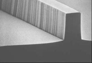
RIE of InP waveguide. Image Credit: Oxford Instruments Plasma Technology
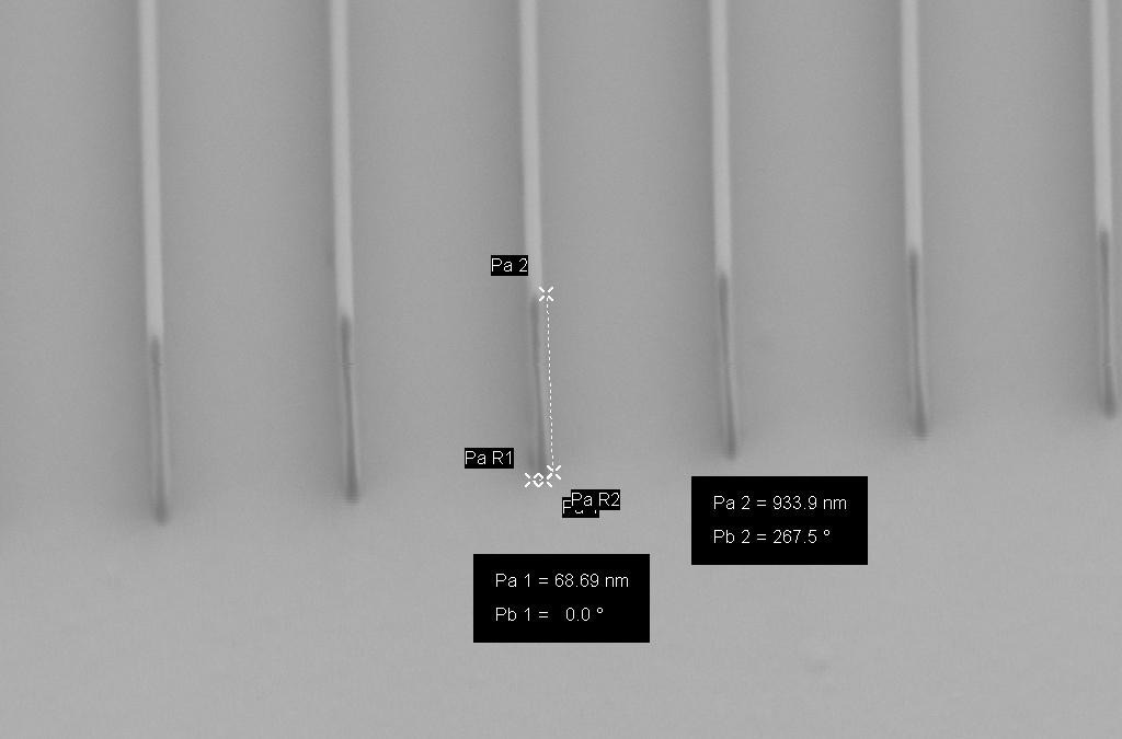
70 nm Fused Silica lines 933 nm deep Cr mask. Image Credit: Courtesy of Cornell Nanoscience facility.
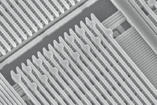
Dielectric metal etch. Image Credit: Courtesy of Atmel
Specifications
Cluster Load Lock Options
- Clusterable with up to 4* process modules, including ALD, ICP, ALE, PECVD, CVD, Ion Beam Etch, and Ion Beam Deposition systems
- Single wafer loading directly into the central handling unit or via an optional load station (needed for through-the-wall integration)
- Multiple chambers can be in operation concurrently where processed wafers wait in the chamber until the load station is under vacuum and empty
*with MX600ss
Typical Conditions
- 5–500 mTorr operating pressure
- 5–200 sccm total gas flow
- 30–800 V DC bias generated on lower electrode
- 0.1–1.5 W/cm2 power density
- The substrate generally sits on a Quartz or graphite coverplate
Advanced Load Lock Options
- Opening: Front held by gas struts with locking mechanism
- Arm position control: Stepper motor
- Wafer tracking: Yes
- Dimensions: Compact dims. +80 mm wider, 90 mm longer. More appropriate for 200 mm wafers
- Recommended for: Where positional accuracy is key to the application
- Not recommended for: Transparent substrates